In the narrative of the semiconductor industry, lithography machines have always been an unavoidable keyword. We have witnessed the evolution of lithography technology from the first generation g-line to the current fifth generation EUV technology, with each technological iteration resembling an ascent of another meter above the snow line of Mount Everest, where the air becomes thinner and the difficulty of climbing increases exponentially.
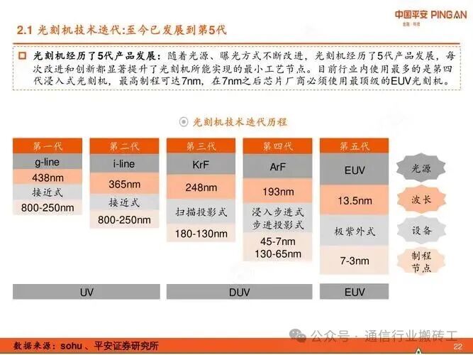
On September 11, a team from Johns Hopkins University published a study in Nature Chemical Engineering that instantly created ripples in both the industry and academia. The paper is titled “Spin-on deposition of amorphous zeolitic imidazolate framework films for lithography applications”. At first glance, it appears to be merely an article about a new material deposition method, but it actually touches on the sharpest pain point in chip manufacturing: In an era where 13.5-nanometer extreme ultraviolet lithography (EUV) has been pushed to its limits, is there a new path that can allow resolution to continue approaching 5 nanometers or even below?
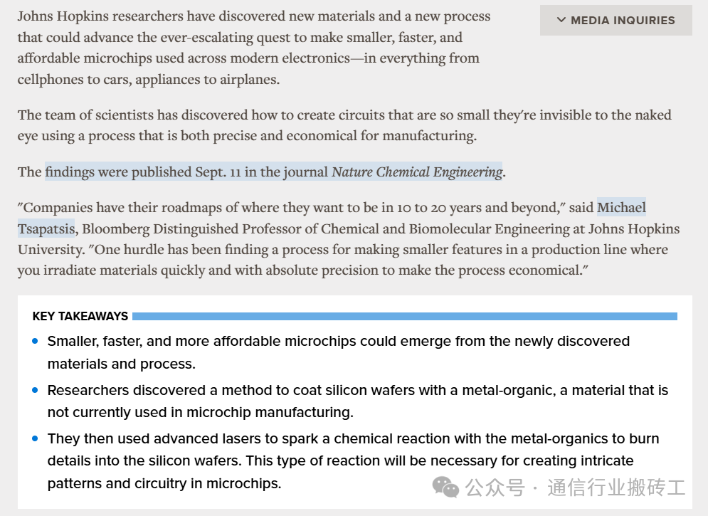
The story begins with a new material. The team proposed a metal-organic film called amorphous zeolitic imidazolate framework (aZIF), and instead of using traditional complex vacuum processes, they spread it on silicon wafers using a method similar to spin-coating photoresist. More intriguingly, this material exhibits excellent absorption and chemical response in the soft X-ray range of 6.5 nanometers, which is key to the so-called “beyond EUV” (B-EUV) route. In other words, if EUV is the asphalt road that the industry has firmly walked on, then B-EUV is the newly opened mountain path in the distance, steep and filled with gravel, but potentially leading directly to higher peaks.
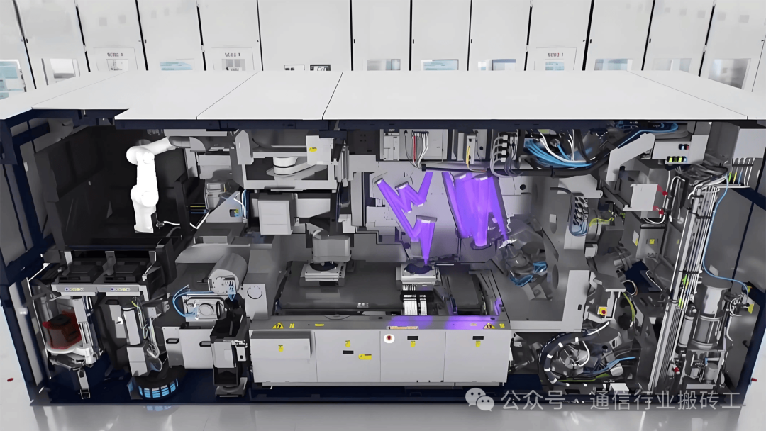
To understand the significance of this breakthrough, one must first discuss the current dilemmas of EUV. Today, the most advanced lithography machines in mass production are all from ASML in the Netherlands, with the 13.5-nanometer EUV light source using tin plasma, and each device costs over $150 million. To continue extending Moore’s Law, ASML is pushing towards high numerical aperture (High-NA) EUV, increasing the NA from 0.33 to 0.55, theoretically compressing the resolution from 13 nanometers to about 8 nanometers. However, the physical limits of this system have already emerged: optical transmittance, mask defects, and random noise are all increasing marginal costs. Even the top wafer fabs need to spend billions of dollars to build specialized clean rooms and supporting environments.
Now, let’s look at the picture of B-EUV. Once the wavelength is shortened to 6.5 nanometers, it means that at the same NA, the resolution can almost be halved, which is an irresistible temptation for any chip manufacturer. However, engineers are well aware that shortening the wavelength is not as simple as just changing a lens in a microscope. The energy loss of a 6.5-nanometer light source is significant, and the stable light power that can currently be generated in the laboratory is far from what is needed for mass production. To support a production line that can produce tens of thousands of wafers per month, stable light source power in the range of tens or even hundreds of watts is required, and the current B-EUV light sources are at least an order of magnitude away from this number. Without sufficient photons, it means low throughput and uncontrollable yield; even if the material is perfect, the factory cannot bear such costs.
The challenges for the optical system are equally severe. At 13.5 nanometers, the industry has achieved about 70% reflectivity with Mo/Si multilayer mirrors, but at 6.5 nanometers, the theoretical combinations of multilayer materials that can be used are extremely limited, with reflectivity dropping to 40% or even lower. This is like a highway charging half the toll for every kilometer; by the time the vehicle reaches the destination, there is hardly any energy left. At 13.5 nanometers, mask defect detection has already become a bottleneck in the industry, while at 6.5 nanometers, every atomic-level protrusion could become a fatal defect, complicating the issues of mask manufacturing and detection. As for the mask pellicle, under EUV, ultra-thin silicon nitride films are barely able to pass, while B-EUV has almost no suitable materials that can transmit light and withstand high-energy radiation.
Under such harsh physical conditions, the research from Johns Hopkins has pressed a key button in the “material” aspect. For the past decade, research on lithography photoresists has been stuck in a “trilemma”: sensitivity, resolution, and random defects are hard to achieve simultaneously. In the conventional chemical system of EUV, the photon absorption rate is low, and to achieve sufficient development contrast, the exposure dose must be increased, but with a higher dose, random noise is amplified, leading to excessive line edge roughness (LWR). The idea behind aZIF is to use metal elements (such as Zn) with a high absorption cross-section to allow short-wavelength photons to release more secondary electrons in the material, thus triggering a more efficient chemical reaction. This has shown higher sensitivity than traditional organic photoresists in experiments at 6.5 nanometers, initially alleviating the conflict between dose and resolution.
More importantly, the preparation method of this material is “spin-coating”, which gives the industry hope for mass production. Today’s photoresists are already accustomed to the process of uniformly spreading via spin-coating, and the solution chemical deposition method (CLD) demonstrated in the paper can not only achieve controllable nanometer-level thickness but also accurately predict deposition rates and film thickness through fluid dynamics modeling. This means that the beautiful results from the laboratory have the opportunity to be extended to large-scale production in wafer fabs. This step is particularly critical for semiconductor manufacturing because no matter how impressive the material’s performance is, if it cannot be achieved uniformly and stably on 300mm wafers, it will ultimately remain in academic papers.
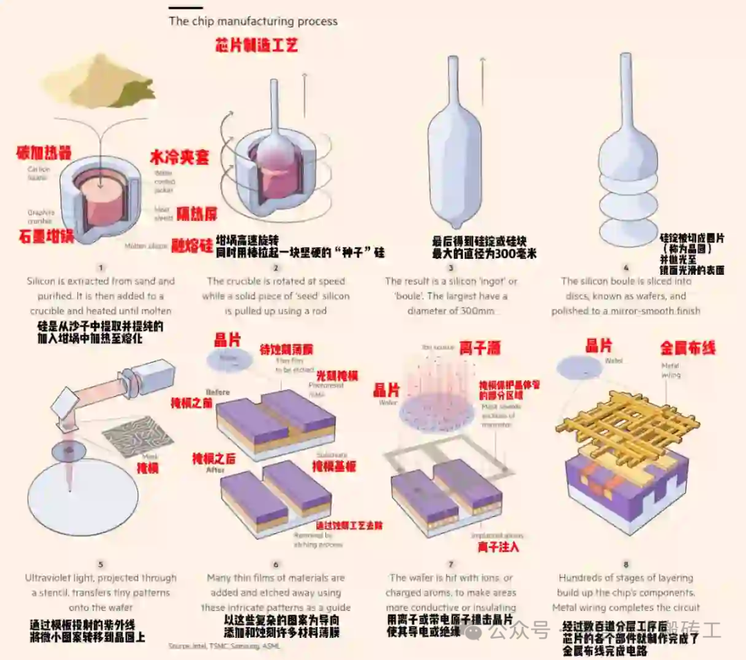
However, a breakthrough in a single material is not enough to rewrite the entire industry’s landscape. Chip manufacturing is a long chain, where light sources, optics, masks, photoresists, etching, and cleaning all need to progress in sync. Even if aZIF performs excellently, if the subsequent etching process cannot adapt, or if metal contamination remains during the cleaning process, the entire process chain will collapse. In fact, these “post-process compatibility” issues are often more difficult to solve than breakthroughs at the front end because they directly relate to yield and reliability, and yield is the lifeline that determines the profitability of a production line.
So the question arises, Will B-EUV replace EUV? If we answer from a timeline perspective, the short-term answer is no. ASML has already achieved the first light of the first High-NA EUV machine in 2024 and will continue to deliver to wafer fabs in 2025. All top manufacturers, including TSMC, Intel, and Samsung, will still focus their investments on High-NA EUV over the next five years. Meanwhile, B-EUV is still at the stage of material research and laboratory exposure validation, with a huge gap to establish a complete toolchain.
In the medium term, B-EUV is not without opportunities. It may become a supplementary tool for certain critical layers. For example, in AI chips or high-performance computing chips, some core layers have extremely stringent linewidth requirements, while other layers can still be completed using EUV or even ArF immersion lithography. If breakthroughs in light sources and optics are achieved within ten years, B-EUV has the chance to “cut in” in specific scenarios, not seeking to replace EUV, but to become a niche technology for high resolution.
In the long term, if all the difficult problems are solved one by one, B-EUV cannot be ruled out as a new mainstream technology. However, this process requires the joint investment of the entire industry chain. Light source manufacturers need to find efficient and stable 6.5-nanometer radiation sources, optical companies need to develop high reflectivity multilayer mirrors, mask manufacturers need to control defects at the atomic level, and the materials science community needs to achieve low randomness and low dose tolerance in resists; the entire ecosystem needs to be rebuilt. In other words, this is a system-level iterative process that will take at least ten years.
The significance of this paper lies precisely in providing a key chip for this iterative process. It does not announce the end of EUV, but proves the feasibility of B-EUV in the material aspect. As Johns Hopkins stated in their official press release, this is a key step in pushing a potential route from fantasy to reality. For the industry, the more pragmatic attitude right now is to continue increasing investment in EUV and High-NA while maintaining a high level of attention to B-EUV at the research level, treating it as a backup plan for the next leap.
Speaking of Moore’s Law in chip manufacturing, it is not just a simple numerical game, but a story of engineers testing the physical boundaries with decades of persistence. Every seemingly impossible breakthrough first flashes in the curves and graphs of the laboratory before gradually seeping into the production line. EUV was once thought to be impossible to mass-produce, yet today it is stably operating in dozens of production lines worldwide. The road for B-EUV is equally arduous, but no one dares to say it will never be realized. The emergence of aZIF material is like lighting a small lamp at the end of a dark tunnel, though faint, it reveals another possibility.
The future of chip manufacturing will not be dominated by a single route, but will resemble a mountain range with multiple peaks. EUV continues to climb steadily, High-NA is opening new heights, while B-EUV is slowly exploring in the distant valley. Ultimately, who can stand on the new peak depends on who can find answers in the four dimensions of physics, chemistry, engineering, and economics simultaneously. For us today, what we can do is closely monitor these small but significant breakthroughs, as they may be the foreshadowing of a turning point in the industry landscape over the next decade.
End of article, thank you for reading. If you liked it, please give it a thumbs up.