Follow and star our public account for exciting content directly.

Source: Online Materials
In modern electronic measurement, communication systems, and biomedical fields, data acquisition and storage of broadband analog signals are often involved for further data processing by computers. To achieve distortion-free acquisition of high-speed analog signals, according to the Nyquist theorem, the sampling frequency must be more than twice the signal frequency. However, in multi-frequency impedance and parameter imaging technology, the anti-noise performance of the orthogonal sequence digital demodulation method is determined by the number of sampling points per cycle of the signal; the more sampling points, the higher the anti-noise performance. When the sampling signal frequency is very high, to sample multiple times within one cycle of the sampled signal, the sampling clock frequency needs to be increased. However, due to the system’s ADC device clock rate not being able to reach the required high frequency or the storage processing speed not meeting the requirements, we can use low-speed ADC devices to perform data acquisition of broadband analog signals through equivalent time sampling, making the system easier to implement.
1. Principle of Equivalent Time Sampling
Equivalent time sampling technology converts periodic or quasi-periodic high-frequency, fast signals into low-frequency, slow signals. The circuit only requires high frequency before sampling, significantly reducing the speed requirements for signal processing and display circuits after sampling transformation, simplifying the overall system design difficulty. Equivalent time sampling is divided into sequential sampling, random sampling, and a hybrid equivalent sampling that combines both methods. This section introduces the sequential sampling in hardware implementation of equivalent time sampling.
Next, I will introduce the hybrid time sampling in equivalent time sampling for periodic signals as shown in Figure 1 (a).
In the first cycle, the clock rising edges at the 2nd and 6th positions on the horizontal axis (time) sample the analog signal, with arrows in the figure indicating the sampling moments. Two points can be collected in one cycle, followed by sampling the analog signal at the 11th and 15th positions of the clock rising edges in the second cycle. For ease of observation, the waveforms from the first to the fifth cycles are arranged vertically. It can be seen that the sampling points in the second cycle are delayed by one clock cycle from the starting point of the first cycle. The sampling points in the third cycle are also delayed by one clock cycle from the starting point of the third cycle. During the fourth cycle, we can find that the second sampling point has already entered the fifth cycle. If we attempt to continue sampling in the fifth cycle, the sampling point in the fifth cycle will be delayed by one clock cycle from the starting point of the fourth cycle, and we will find that the value sampled at the starting point of the fifth cycle is a repeat of the value sampled in the first cycle. Therefore, we can terminate the sampling, and we obtain the 6th waveform as shown in Figure 1, representing the 8 data points sampled from one cycle of the sine wave.
The theoretical basis for collecting multiple points in each cycle during equivalent time sampling is provided, as well as the theoretical basis for collecting a single point in each cycle.
We achieve or approach the processing speed clock requirements by frequency dividing the high-frequency clock. In Figure 1 (b), the clock signal with the minimum amplitude is the sampling clock. It can be clearly seen from Figure 1 (b) that the clock waveform after frequency division samples the signal at the rising edge of the clock, resulting in the equivalent time sampling as shown in Figure 1 (a).
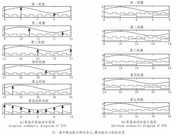
Figure 1 Equivalent Time Sampling Diagram
2. Implementation of Equivalent Time Sampling Based on FPGA
2.1 System Hardware Implementation Block Diagram
The overall block diagram of the system is shown in Figure 2. The equivalent sampling clock controlled by the FPGA is connected to the clock part of the ADC device, which samples the broadband analog signal under the control of the clock. The collected data is transmitted to the FIFO in the FPGA, which then passes the data from the FIFO in the FPGA to the FIFO in the USB, and the USB pushes the FIFO data to the computer, where the received data undergoes reconstruction processing. For obtaining the signal cycle, in multi-frequency impedance and parameter imaging technology, the cycle of the collected signal is determined by the cycle of the transmitted signal, while the cycle of other complex periodic signals can be obtained through the adopted method.
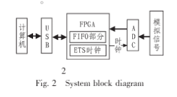
Figure 2 System Scheme Block Diagram
2.2 Program Implementation of Equivalent Time Sampling Clock
Figure 3 shows the input and output ports of the equivalent time sampling module generated based on FPGA. CLK represents the input of the high-frequency clock, RESET represents the reset input, FREN_CON represents the frequency division control input used to control the frequency division number of the high-frequency clock, SANM_CONT represents the period of the analog signal containing how many high-frequency clock signal waveforms, and CLK_ADC_OUT represents the output clock port, which is connected to the clock input port of the analog-to-digital converter (ADC).
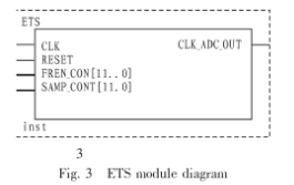
Figure 3 Equivalent Time Sampling Module Diagram
Below is the code required to implement the clock for equivalent time sampling:
SIGNAL SAMP_CONTS:STD_LOGIC_VECTOR (11 DOWNTO 0) := (OTHERS => '0');
SIGNAL ADC_CLK_BANK:STD_LOGIC_VECTOR (11 DOWNTO 0) := (OTHERS => '0');
SIGNAL CLK_CNT: INTEGER RANGE 0 TO 5000 := 0;
SIGNAL CLK_TANK: STD_LOGIC := '0';
SIGNAL EN: STD_LOGIC := '1';
BEGIN
PROCESS (CLK, RESET)
BEGIN
IF RESET = '1' THEN
EN <= '0';
SAMP_CONTS <= '0';
END IF;
3. Waveform Simulation
The waveform simulation in Figure 4 assumes that one cycle of the analog signal equals 8 CLK clock cycles, and CLK_ADC_OUT is a 4-frequency division of CLK with a 50% duty cycle. The rising edge of the clock indicated by arrow 1 marks the end of the first cycle, and after the rising edge, it enters the second cycle. Similarly, the rising edge of the clock indicated by arrow 2 marks the end of the second cycle, and after the rising edge, it marks the entry into the third cycle.
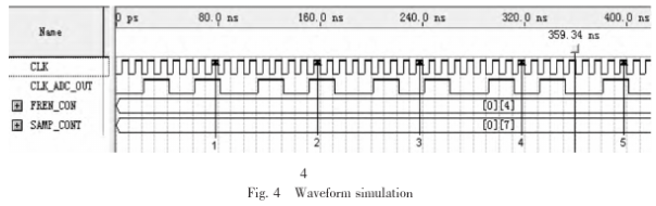
Figure 4 Waveform Simulation
In the first cycle, timing starts from the first rising edge of CLK while simultaneously frequency dividing CLK to obtain the CLK_ADC_OUT clock signal. In the first cycle, at the second rising edge of CLK, the CLK_ADC_OUT level flips (with a delay). In the second cycle, at the third rising edge, the CLK_ADC_OUT level flips, and in the third cycle, at the fourth rising edge of CLK, the CLK_ADC_OUT level flips. It can be seen that the waveform simulation diagram expresses the clock implementation of Figures 1 (a) and (b). It should be noted that although there are also 8 rising edges of CLK in the first cycle, it does not represent the waveform between the rising edge of CLK indicated by arrow 1 and the first rising edge of CLK in the second cycle.
4. Conclusion
This article introduces the basic principles of equivalent time sampling and the specific implementation scheme of the system. The equivalent time sampling technology enables the use of low-speed ADC devices for the acquisition of broadband analog signals, reducing the requirements on ADC devices and the complexity of system implementation. The equivalent time sampling technology introduced in this article, due to the use of FPGA sampling technology, significantly improves the ability to collect multiple points within one cycle of the sampled signal compared to sequential equivalent time sampling, which can only collect one point per cycle, and allows control over the number of sampling points within one cycle of the collected signal, thus enabling variable frequency control sampling based on subsequent device processing speeds. By implementing equivalent time sampling through FPGA, the complexity of system implementation is reduced, and the code can be easily modified, making system debugging more convenient.
*Disclaimer: This article is original by the author. The content of the article reflects the author’s personal views, and reprinting is only to convey a different perspective, not to express agreement or support for that view. If there are any objections, please feel free to contact.
‧‧‧‧‧‧‧‧‧‧‧‧‧‧‧ END ‧‧‧‧‧‧‧‧‧‧‧‧‧‧‧‧Follow the WeChat public account “ZYNQ”, reply “join group” to join the FPGA/ZYNQ technology exchange group. Reply “m” in the background to see more exciting content.