1: FPGA and Productivity
FPGA is known as a universal chip that can achieve almost any function through logic programming. For more details, refer to “Talking about FPGA – ‘The Universal Chip?'”.
So the question arises, how difficult is it to use FPGA to accelerate artificial intelligence and implement deep learning algorithms?
It is quite challenging!
If we start from the AI algorithm, then begin coding in Verilog, debugging, optimizing, and finally downloading it to the FPGA for operation, it requires a lot of manpower and resources. Without at least a year and a half, it is hard to achieve results.
However,
if there is an FPGA app library containing various AI applications, you can download the corresponding programs to the FPGA, as shown in the figure below:
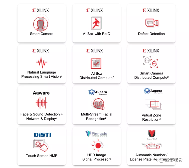
There are smart cameras for face recognition, defect detection, ReID (pedestrian detection/tracking technology), voice recognition, multi-target face recognition, intelligent driving assistance, etc.
These applications can be directly compiled and downloaded to the FPGA, simplifying the development process based on existing applications, achieving an “immediate use” effect.
This can quickly form productivity.
Even if there are custom requirements, the feasibility of the route can be quickly assessed, allowing for secondary development based on that.
This approach is faster and more efficient than starting directly from Verilog coding.
So how does this work?
2: How to Do It
What steps are needed to build a face recognition system using FPGA?
If using the KV260 equipped with Zynq UltraScale+ FPGA, it takes a total of three steps:
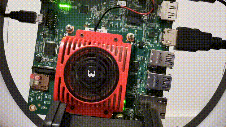
Step 1: Assemble the Components:
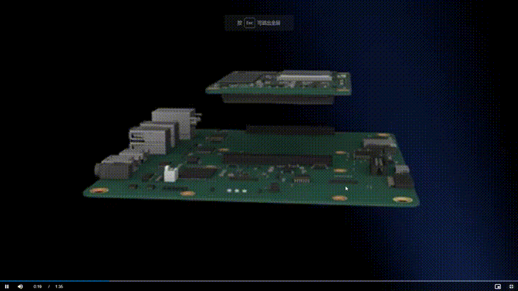
KV260 is an FPGA system based on Zynq UltraScale+, which includes resources such as CPU, FPGA, GPU, etc.
Under the red heat sink is the Zynq UltraScale+ chip. It has a quad-core A53 processor and an FPGA with 256K logic cells, representing a “dual-sword combined” architecture.
The components include:
1: Power supply: for system power.
2: SD card: for burning the operating system.
3: Camera: for video input.
4: USB to serial cable: for system serial output.
5: Ethernet cable: for internet connection to download smart applications.
6: HDMI cable: for video output.
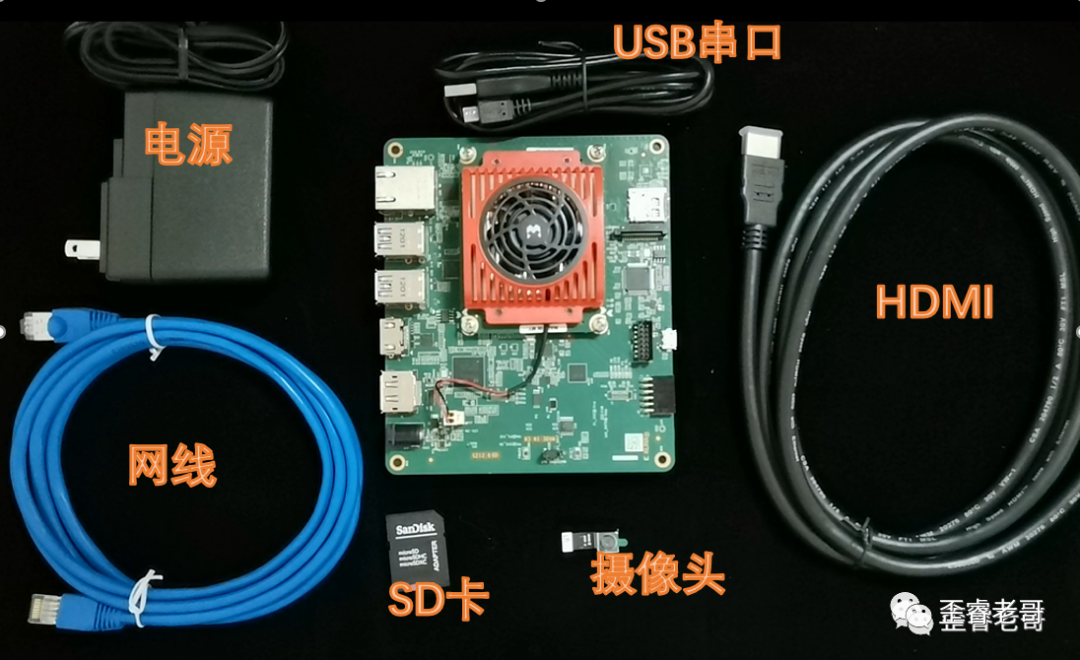
Then assemble these components together.
Step 2: Download the Application
1: Download the Linux system to the TF card, insert the TF card, and power on to start Linux.
2: Connect the Ethernet cable and check the connectivity; you can ping the gateway to see if the connection is successful.
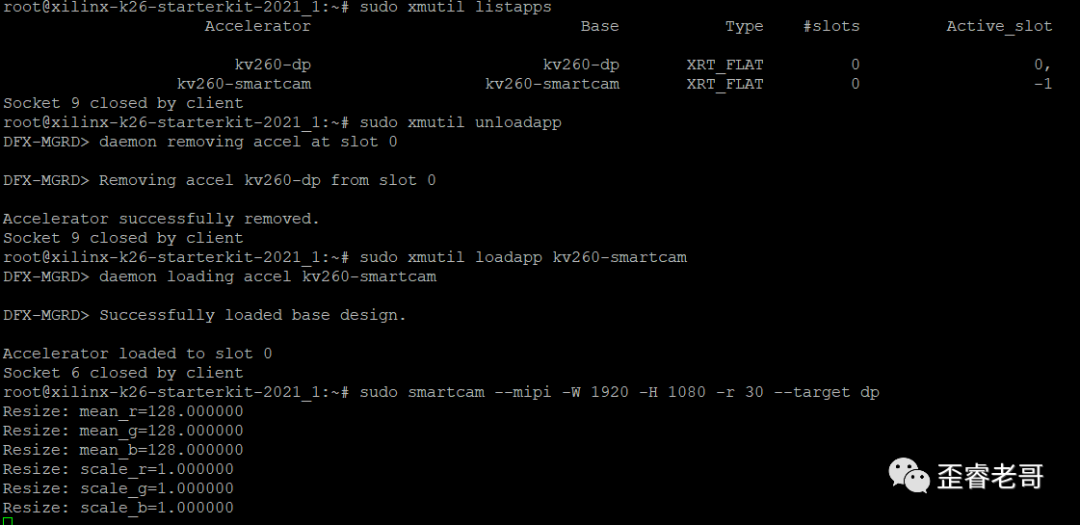
3: Once online, directly select and install the corresponding application, which is the smart camera capable of face recognition.
The following image shows the download and installation of the application. After clicking the download command, make sure to download in root mode,sudo dnf install packagegroup-kv260-smartcam.
The installation time is a bit long; once installed, let it run for a while.

Step 3: Start Testing
Start the application and begin testing. Mount the application in the Linux system, then start the AI application.
sudo smartcam -mipi -W 1920 -H 1080 -r 30 –target dp
This is somewhat akin to the steps involved in putting an elephant in a refrigerator!
So, how does it perform?
3: How is the Performance?
This is how it looks.
I used this FPGA system mounted on a live streaming pole, paired with a monitor, making it look somewhat like a live streaming studio based on an industrial camera.
With this “live streaming studio”, I checked it out, and there was no beauty effect.
So, no live streaming.
How does the AI perform?
I showed the KV260 a video of the UEFA Euro Cup award ceremony.
Why the UEFA Cup award? Mainly because there are many people appearing in this video simultaneously, and the scene is constantly moving. I wanted to test the processing capability of this system.
1: The Number of Faces Recognized.
2: Processing Latency.
Videos with two or three people cannot test the capabilities of this AI chip.
Moreover, if the scene is static, there are no high latency requirements. For instance, face recognition at a community entrance will feel noticeably delayed.
So, can we see how many faces the KV260 can recognize in the video?

This match is the UEFA Cup award ceremony, and you can see that the KV260 immediately recognized all the faces of the winning team members.
The efficiency is very high.
I counted, and at most, 22 faces were recognized and captured simultaneously. Both the main players and substitutes were captured.
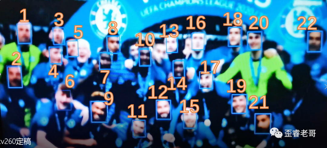
Being able to capture 22 faces simultaneously also reflects the face recognition capability of this chip.
Moreover, the scene is continuously switching, and the latency control is quite good, although it is difficult to quantify.
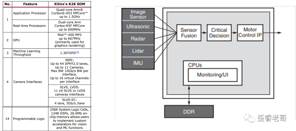
4: System and Principles
Having seen the performance of the FPGA in this system, let’s get into some technical details.
What components are needed for an AI chip system?
CPU System: Responsible for OS operation, system initialization, data flow control, signal transmission, peripheral management, etc.
DPU System: (Deep Learning Processor Unit) responsible for accelerating deep learning algorithms, serving as an intelligent acceleration engine.
In simple terms: two parts, control and computation.
This is the classic CPU + FPGA solution, widely used in many embedded industrial fields, typically ARM + FPGA;
ARM is responsible for control management and peripheral management, while FPGA is responsible for AI acceleration.
The Zynq UltraScale+ integrates both into a single chip, as shown in the diagram below.
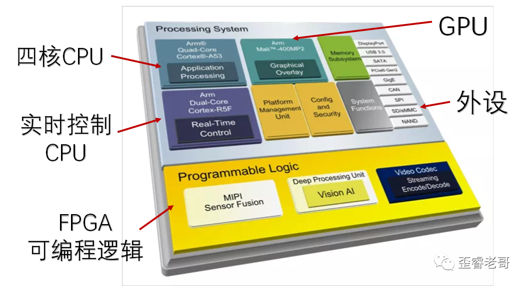
Its main resources include: quad-core CPU A53, a Mali GPU, and support for real-time CPU, dual-core R5F.
The term DPU reminds us of Xilinx’s acquisition of Deep Vision Technology, which had a significant impact in the industry.
At that time, Deep Vision’s core technology was based on FPGA DPU technology, claiming to compress neural networks by dozens of times without affecting accuracy, and to use “on-chip storage” to store deep learning algorithm models, reducing memory reads and significantly lowering power consumption.
Looking at it now, it is uncertain whether the technology implemented in the Zynq UltraScale+ chip is a continuation of that legacy, but its performance is still strong.
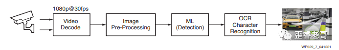
The main workflow and performance indicators are shown in the diagram below:
It supports 11 MIPI cameras, which should be sufficient for the number of cameras needed in a vehicle.
In any case, this chip supporting so many cameras is, to my knowledge, the most I have seen.
Moreover, the most important aspect is that this chip has a rich set of FPGA programmable resources: 256K logic cells; (logic cells consist of LUT and REG). It operates at 333MHz, and its programmable logic’s deep learning processor DPU capability reaches 1.3 Tops.
In addition to smart cameras, there are other applications available for different use cases.
For example, intelligent driving, voice recognition, security detection, etc.
Here, I want to emphasize ADAS (Advanced Driver Assistance Systems), which utilize various sensors installed in the vehicle to collect environmental data inside and outside the vehicle in real-time, performing technical processing for identifying, detecting, and tracking static and dynamic objects. This allows drivers to quickly notice potential dangers, enhancing safety through proactive safety technologies. This includes driver fatigue warnings and identity recognition, with face recognition being essential for personalized driving cabins in passenger vehicles, as well as future business models. Some prototypes are already in development.
To summarize:
1: Processing Capability: The KV260 uses the Zynq UltraScale+ MPSoC chip, which has a quad-core application processor, GPU, real-time processor, and 256K LC FPGA, providing sufficient hardware resources to handle AI applications.
2: Peripheral Interfaces: The KV260 supports 11 camera inputs, capable of supporting applications like ADAS (Advanced Driver Assistance Systems).
3: Software Support: In addition to hardware, there are many software packages available, such as face recognition, intrusion detection, autonomous driving, etc., facilitating secondary development.
FPGA can achieve millisecond-level applications through deep learning, with high throughput and low latency, which may be an advantage.
The earlier face recognition test, which recognized 22 faces simultaneously, also indirectly indicates a high number of face recognitions with low latency.
Why 22 faces? Because the video I found contained exactly 22 faces.
Of course, this test only provides a visually perceptible perspective. Actual applications can be tested according to requirements, and evaluations can be made based on test results to accelerate the design-in process.
Click “Read Original” to see the complete video.
Welcome to follow: Yai Rui Lao Ge. If you find this article good, feel free to like, share, and comment.
Previous Readings:
Mastering “Core Technology” is Just Gaining Entry into the Game
How Did the 5nm and 7nm Chip Processes Come About?
From Human Training AI to AI Training AI, How Far Is the Road?
The “Jargon” of High-Quality Chip Engineers
Why Have Chip Engineers Become So Expensive?
Talking about FPGA – ‘The Universal Chip?’
Talking about DPU – From Network to Data
Unveiling the “Secrets” Behind Chip Processes and Moore’s Law