
Click the “blue words” above to follow for more exciting content.
This article contains a total of 3718 words, and reading the full text will take about 9 minutes.
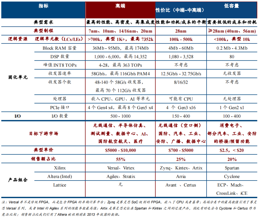
(1) Process Technology is a distinguishing standard for each generation of FPGA and is the primary metric for evaluating FPGA. As a type of digital chip, FPGA follows Moore’s Law, with new generations of products typically released every 2-3 years. Utilizing more advanced processes can reduce power consumption, chip size, and unit cost, resulting in the performance of new generation FPGA products generally surpassing that of the previous generation. Therefore, the process technology is the first consideration when evaluating an FPGA. Another reason why process technology is crucial for FPGA is that they are often used as tools for large-scale ASIC/ASSP prototyping, thus they must keep up with the most advanced processes.(2) The number of Logic Units represents the basic capacity of the FPGA and is currently the unified metric for evaluating FPGA capacity. The minimum functional unit of an ASIC is a “gate,” and its capacity is measured in gate count. The minimum functional unit of an FPGA is called a Basic Logic Unit (referred to as BLE in academia; FPGA manufacturers call it a Logic Cell), which includes one LUT and one register. The programmable basis of FPGA is the LUT, which can implement combinational circuits, and when combined with registers, can complete sequential circuits, meaning that a logic unit has the capability to perform all digital circuit functions. Therefore, the more logic units, the larger the FPGA capacity, allowing for the construction of larger and more complex circuits.High-capacity FPGA directly reflects the capabilities of FPGA manufacturers, with only a handful of manufacturers able to continuously supply them. Large FPGA logic unit counts are generally above 1 million, as exceeding this number requires changes to the FPGA architecture, including LUTs, CLBs, and interconnections; otherwise, power consumption and delay would become unacceptable. Additionally, EDA tools must support design processes and layout routing algorithms must be iterated. Thus, the design difficulty of high-capacity FPGAs far exceeds that of medium and low-capacity FPGAs. The presence of large FPGA products often directly reflects the capabilities of FPGA manufacturers, with only a few able to achieve this. Currently, among the top five FPGA manufacturers globally, only Xilinx and Altera (Intel) have the capability to continuously provide a large-capacity FPGA product line. In the past, FPGA manufacturers used gate count to measure FPGA capacity, but since 2000, they have gradually shifted to the unified metric of “logic unit count” because: 1) Gate count is an indirect indicator of FPGA capacity, while logic unit count is a direct indicator. In the late 1990s, FPGAs were comparable to gate arrays in terms of gate count, making it unnecessary to convert to a competitor’s evaluation metric; 2) With the increase in FPGA integration, continuously embedding RAM, DSP, CPU, and other functions into FPGAs, as well as the transition from LUT4 to LUT6, LUT8, and even higher, it has become increasingly difficult to convert FPGA capacity into gate count. (The “logic unit count” metric better represents the number of resources available for FPGA use. The conversion method: compare the basic units of FPGA (such as LUT+FF, ESB/BRAM) with standard gate arrays that perform the same function, the number of gates in the gate array represents the equivalent gate count of the FPGA basic unit, and then multiply by the number of basic units to obtain an estimated gate count for the FPGA.)*Taking Xilinx as an example, its logic unit count is based on “1 LUT4 + 1 register” because, in the early FPGAs, a logic unit indeed contained only 1 LUT4, 1 register (and several MUXes), so the logic unit count equaled the number of its LUTs. However, with the introduction of LUT6, the addition of carry chains, and the increase in the number of MUXes, a single logic unit can now perform the functions that previously required multiple LUT4s and registers. Therefore, the current logic unit count metric often equates internal logic resources to the number of “LUT4 *1 + register *1,” with the specific multiplier determined by each company. For Xilinx, its 7 series products use a multiplier of 1.6 for the internal LUT6 count, as in the 7 series architecture, one LUT6 connects to 2 registers, making the register count 2/1.6 = 1.25 times the logic unit count.Currently, gate count is often used as one of the performance indicators for FPGAs, representing the potential that can be developed with the FPGA. The larger the gate count, the more functions users can develop and the more problems they can solve when using the FPGA.(3) The performance of hardened units represented by BRAM (Block Random Access Memory), DSP (Digital Signal Processor), and transceivers is the second major part of the FPGA performance system. In addition to programmable logic units, modern FPGAs also integrate many hardened units. The commonly discussed SerDes rates of FPGAs, DSP operating frequencies, etc., all refer to the performance of different hardened units within the FPGA.Incorporating discrete DSP and other devices onto the FPGA is driven by the need to reduce circuit area and power consumption. In the mid-1990s, FPGA manufacturers discovered that users frequently used LUTs as storage (i.e., “soft” implementation), occupying many logic units and leading to insufficient FPGA capacity. Therefore, RAM was the first unit to be hardened into the FPGA, i.e., “hard-cored.” By embedding these frequently used functions into the FPGA, computational efficiency can be greatly improved, and users do not need to worry about wasting precious logic resources. For example, embedding DSP into the FPGA (instead of implementing it through versatile LUTs) can save 80% of power consumption and the area occupied by DSP on the board. Thus, after surpassing gate count in the late 1990s, the competitive focus of FPGA manufacturers shifted from gate count to integration competition, embedding many functions such as RAM, DSP, transceivers, DDR interfaces, CPUs, and GPUs into FPGAs, which is why modern FPGAs often contain many hardened units. Therefore, performance evaluation metrics for FPGAs often involve these hardened units.DSP Operating Frequency: The higher the DSP operating frequency, the faster the data computation speed, typically measured in megahertz (MHz).SerDes Rate: The SerDes rate of an FPGA directly reflects its ability to communicate with the outside world. Entering the information society, the explosion of digital information has led to an explosive increase in the amount of data that hardware must carry. While improving the data processing capabilities of device systems, it is also necessary to enhance their data transmission capabilities to avoid data congestion caused by large amounts of data waiting to be processed. The higher the rate, the larger the data transmission volume, typically measured in Gbps.DDR Rate: Refers to the standard rate of data reading interfaces for DDR2/DDR3/DDR4/DDR5 synchronous dynamic random access memory, measured in MT/s.(4) Nevertheless, an “excellent” FPGA is not necessarily the most capable but rather the one that best meets the user’s needs, achieving optimal performance across multiple metrics such as power consumption, hardened functions, and cost. This is because FPGA users purchase the entire chip, and if it integrates too many unnecessary functions, it effectively increases the usage cost. Therefore, FPGA manufacturers are segmenting their products based on various downstream markets/application scenarios, offering corresponding high, medium, and low-end products. Taking the leading Xilinx as an example, it has high-end Virtex, cost-effective Kintex, low-capacity Spartan, ultra-low power CoolRunner, and with differences in temperature and speed grades, there are over 1000 part numbers in just the 7 series product line, making the product matrix very complete.① For the high-end market, the demand is for the highest performance, and the unit price is also very expensive. High-end FPGA demand comes from wireless communication, such as the baseband and core network sides of 5G communication, as well as artificial intelligence algorithm training, semiconductor prototype chip simulation, spacecraft main systems, communication testing instruments, and medical imaging instruments. These scenarios typically involve large data processing volumes or require extremely low latency and high computing power, or need very strong radiation resistance. Currently, high-end FPGA processes are generally at 20nm and below, with logic unit counts greater than 700k, typically above 1 million, not only with an astonishing number of DSP and BRAM but also with transceiver rates generally above 50GB/s, while also integrating processing units like CPUs and advanced interfaces like PCIe 5, essentially appearing in SoC form. Currently, high-end FPGAs are primarily provided by Xilinx or Altera, with representative products including Xilinx’s 7nm ACAP Versal, 16nm Virtex Ultrascale+, Altera’s 10nm (Intel 7) Stratix 10, and Agilex, which are typically very expensive, with unit prices ranging from $5,000 to $10,000, reflecting the highest levels of contemporary FPGA performance, density, and integration. The high-end market is the most important source of revenue for FPGA manufacturers, with Altera’s high-end FPGA product Stratix series accounting for as much as 55% of its revenue.② The mid-range market seeks cost-effectiveness, requiring a balance between performance and cost. Demand comes from the air interface side of wireless communication, industrial, security, and defense scenarios, where the required logic unit counts are typically between 100k and 500k, with transceiver rates around 25Gb/s, and the typical process is 28nm, making it the backbone of the FPGA industry. The mid-range market does not pursue the highest performance; performance and power consumption are equally important. Typical mid-to-high-end products include Xilinx’s Kintex and SoC FPGA Zynq, Altera’s Arria, and Lattice’s latest Avant, while the mid-to-low-end market includes Xilinx’s Artix and Lattice’s Certus. Generally, the revenue share is around 25%. Unit prices typically range from several tens to several hundred dollars, not exceeding $5,000.③ The low-capacity market has lower performance requirements but needs extremely low cost and power consumption. Low-capacity FPGAs are commonly found in consumer electronics, some automotive and industrial IoT scenarios, with the most typical applications being bridging in video devices, including interfaces for MIPI, DPI, CMOS cameras, displays, etc. Nowadays, VR and AR devices also utilize them. Since low-capacity FPGAs are generally used as flexible interfaces or reserved for future use, they do not require high density, typically around 5k-10k capacity is sufficient, and they generally do not need transceivers, processors, or other complex functions. Nevertheless, due to the majority of low-capacity applications being in mobile devices, there are very high requirements for cost and power consumption, typically in the range of 5mW-150mW, with unit prices not exceeding $20 per chip, and typical prices around $2.5 per chip.
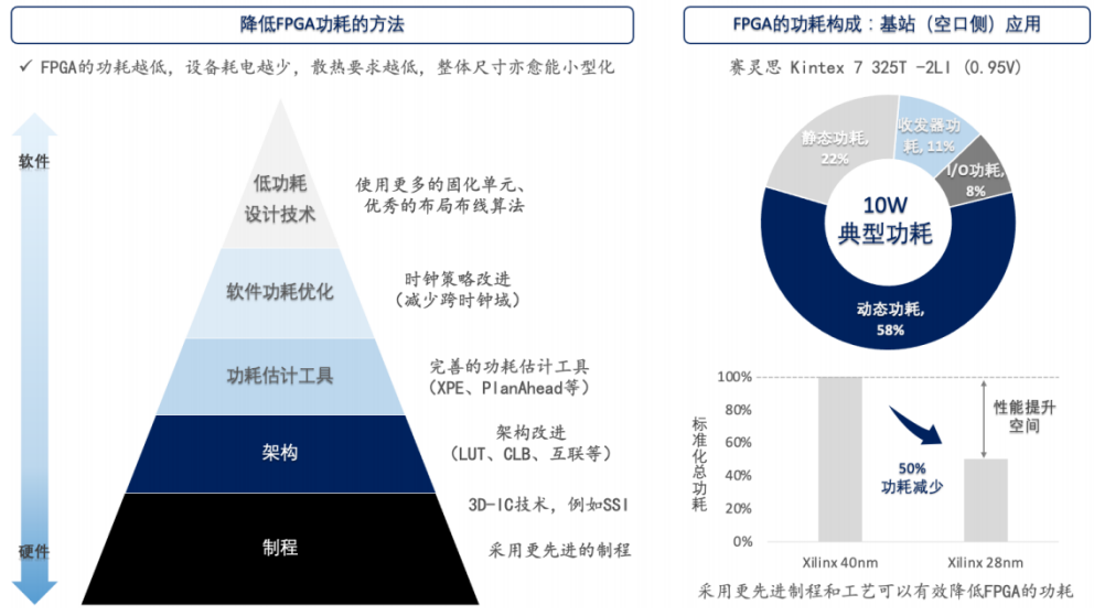
The total power consumption of an FPGA consists of static power consumption, dynamic power consumption, IO power consumption, and transceiver power consumption. Static power consumption is the power consumed by the circuit, mainly caused by transistor leakage; dynamic power consumption refers to the power consumed by circuit switching when the chip is in operation, originating from clock, logic, BRAM, processing units, transceivers, and other units. The lower the chip power consumption, the less power the device consumes, and the lower the heat dissipation requirements (or no additional heat dissipation modifications are needed), allowing for further miniaturization of the overall size. Generally speaking, embedded processing places great emphasis on power consumption, with a power budget not exceeding 50W. FPGA companies reduce power consumption in two ways: 1) Hardware-wise, by using more advanced processes and technologies, 3D-IC technology, embedding more hardened units, and adopting lower power architectures; 2) Software-wise, by optimizing layout algorithms to reduce the occupation of cross-clock domains and redundant logic resources, as well as providing power estimation tools to facilitate user modifications. Therefore, many manufacturers are exploring new paths in power consumption to establish competitive advantages in the low-capacity market, thereby breaking free from the traditional competition based solely on high volume and low cost, as well as the ongoing issue of price wars. The low-capacity market is technically mature, with relatively low entry barriers, and the products offered by manufacturers often have little differentiation, making price wars common. However, due to the persistent contradiction of “performance-power consumption-portability,” the pursuit of low power consumption in the low-capacity market is also continuously growing. Therefore, the ability to optimize power consumption is a key competitive advantage for low-capacity market manufacturers beyond price. For example, the global leading FPGA manufacturer Lattice, whose Certus series uses FD-SOI technology, has power consumption that is 70%-75% lower than CMOS-based competitors, such as Altera’s Cyclone and Xilinx’s Artix. Thus, although Lattice holds only 5% of the global FPGA market share and lacks a large-capacity FPGA product line, its advantage in power consumption gives it a significant edge in the low-capacity market, allowing it to achieve overall gross margins of over 50%.

Risk Warning: This content only represents the analysis, speculation, and judgment of the Breaking Research team, and is published here solely for the purpose of conveying information, not as a basis for specific investment targets. Investment carries risks; please proceed with caution!Copyright Statement: The copyright of this content belongs to the original party or author. If reproduced, please indicate the source and author, retain the original title and the integrity of the article content, and bear legal responsibilities such as copyright.
END
