Welcome FPGA engineers to join the official WeChat technical group
Clickthe blue textto follow our FPGA home – the best and largest pure FPGA engineer community in China

JTAG (Joint Test Action Group) is an interface, and a group called the JTAG group was established for this interface in 1985. In 1990, IEEE felt everything was in order and thus released IEEE Standard 1149.1-1990, named the Standard Test Access Port and Boundary-Scan Architecture, which is the famous JTAG.
Do you know the three main functions of JTAG? They are quite significant:
1. Downloader, which downloads software to FLASH.
2. DEBUG, similar to a doctor’s stethoscope, it can listen to the internal thoughts of the chip.
3. Boundary scan, which can access the logical state of internal signals of the chip, as well as the state of chip pins, etc.
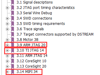
JTAG does not have a standard interface definition; even each company’s definition is different. In the ARM “System and Interface Design Reference” document
Document download link:
Link: https://pan.baidu.com/s/13aQXOXR73_wiERz2kwN15w
Extraction code: xaaf
(Tip: The public account does not support external links, please copy the link to the browser for download)
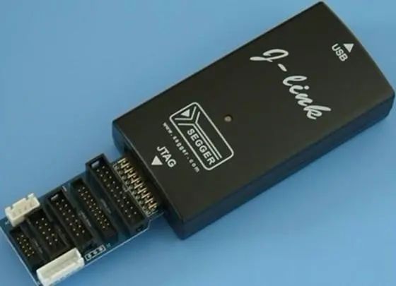
What we often see on the Internet is the JTAG interface of SEGGER company’s Jlink.
J-Link is a debugger based on JTAG, introduced by the German SEGGER company. Simply put, it is a JTAG protocol converter box, which is a small USB to JTAG converter box, connected to the computer via USB, while the connection to the target board is still through the jtag protocol. It accomplishes the task of converting from software to hardware.
At the same time, Jlink is also considered the most popular debugger. Through the “System and Interface Design Reference”, it can be seen that this ARM official JTAG20pin is not the same.
Here, I hope everyone understands the relationship between ARM, Jlink, and JTAG.
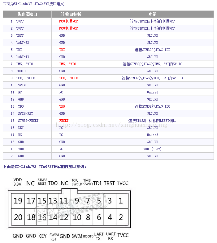
The ST-link V2 interface is also used quite frequently. As mentioned above, this is also an interface defined by the ST company, as shown below:
Ulink, CMSIS_DAP, and other STM32 debuggers follow the same principle.
Boundary Testing:
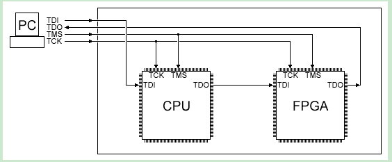
For example, if you have two chips that are connected by many lines, how can you ensure that the connections between these lines are OK? Use JTAG, which can control all IC pins. This is called chip boundary testing.
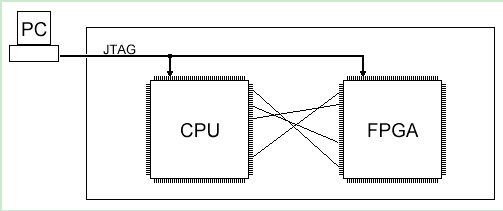
In the JTAG interface, the most commonly used signals are four: TCK/TMS/TDO/TDI. The JTAG interface can be used in a one-to-one manner, or can form a daisy chain in a one-to-many topology, as shown in the diagrams below. In multi-core chips, the internal chip connections are already in a daisy chain format.
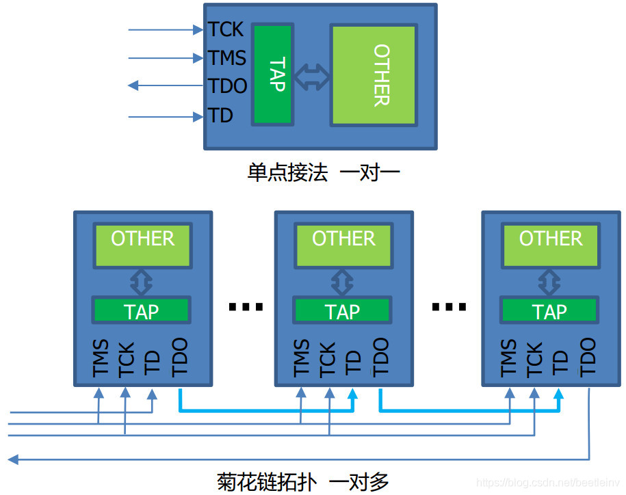
JTAG daisy chains have many applications
CPU and FPGA manufacturers allow JTAG to be used for port debug; FPGA manufacturers allow configuration of FPGA through JTAG, using JTAG signals to enter the FPGA core.
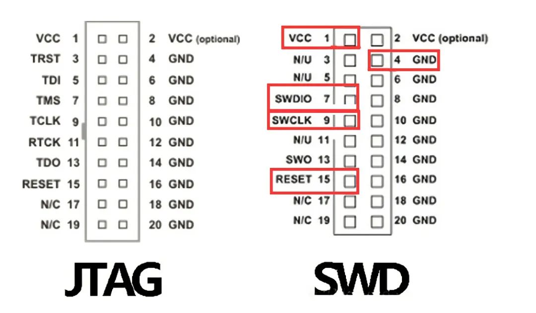
SWD interface: Serial Wire Debug, which can be considered a different debugging mode compared to JTAG, is most directly reflected in the debugging interface. In comparison to the JTAG with 20 pins, SWD only requires 4 (or 5) pins.
VCC, SWDIO, SWCLK, GND (in some cases, the RESET pin is also added).
Differences between SWD and traditional debugging methods:
-
SWD mode is more reliable than JTAG in high-speed mode. In cases of large data volumes, JTAG program downloads may fail, but the occurrence is much less likely with SWD. Generally, when using JTAG emulation mode, you can directly use SWD mode as long as your emulator supports it, so it is recommended to use this mode.
-
When the CPU‘s GPIO pins are insufficient, you can use SWD emulation, which supports fewer pins.
-
When the hardware PCB has limited size, it is recommended to use SWD mode, which requires fewer pins and thus less PCB space, allowing for the selection of a very small 2.54 pitch 5 pin terminal as the emulation interface.
In the Keil environment, the Jlink debugger’s JTAG mode and SWD mode
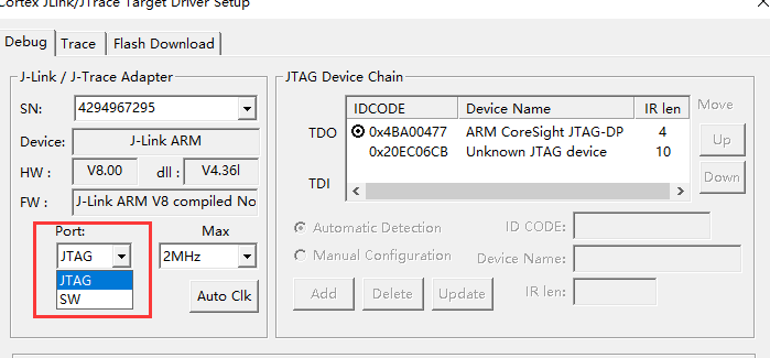
In the IAR environment, the Jlink debugger’s JTAG mode and SWD mode
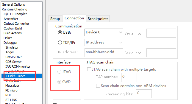
Comparison chart between Jlink ‘s JTAG mode and SWD mode
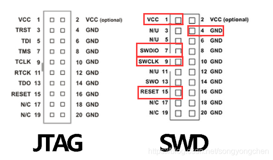
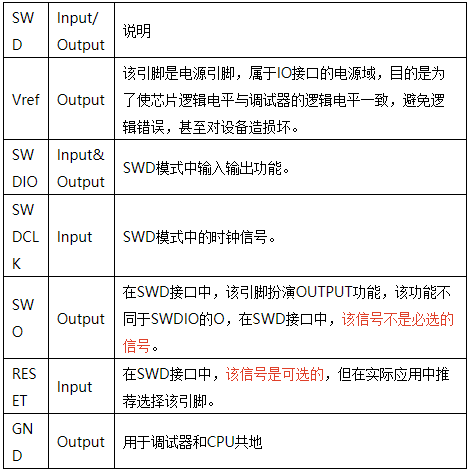
JTAG pin description
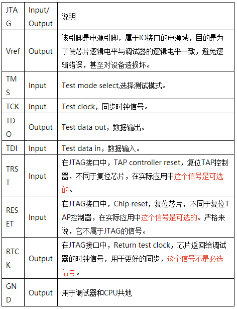
SWD pin description
As mentioned above, the Vref pin belongs to the power domain of the IO interface, aimed at ensuring that the chip’s logic level matches the debugger’s logic level to avoid logical errors and even damage to the device.
There is a jumper cap for Vref on the Jlink.
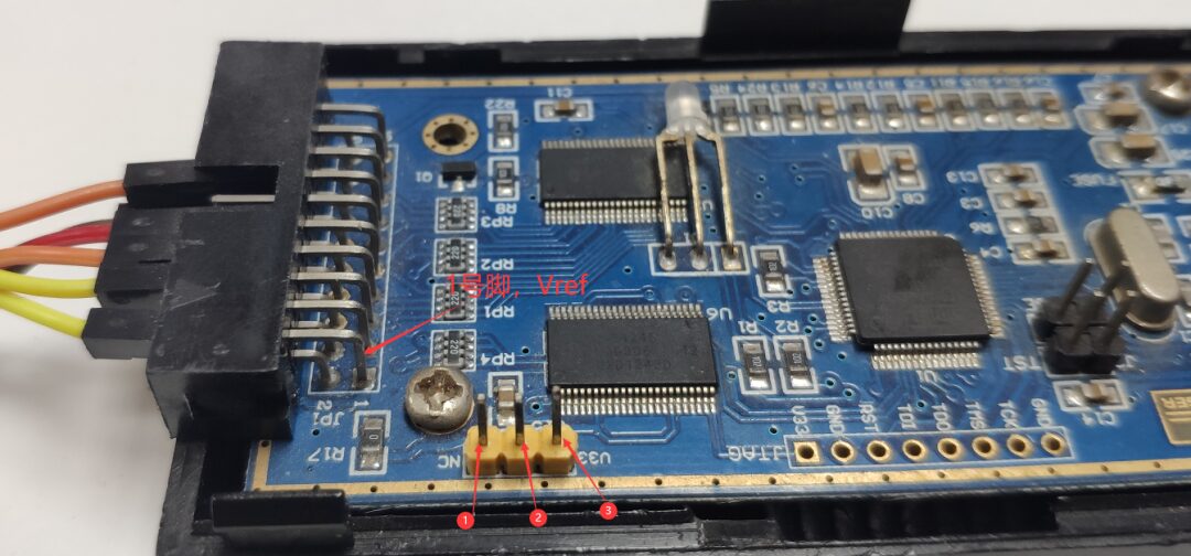
Three pin headers: ① is NC, ② is Vref, connected to the output’s 1 pin, ③ is 3.3V
If you want the Jlink ‘s 1 pin Vref output to be 3.3V, just short connect ② and ③.
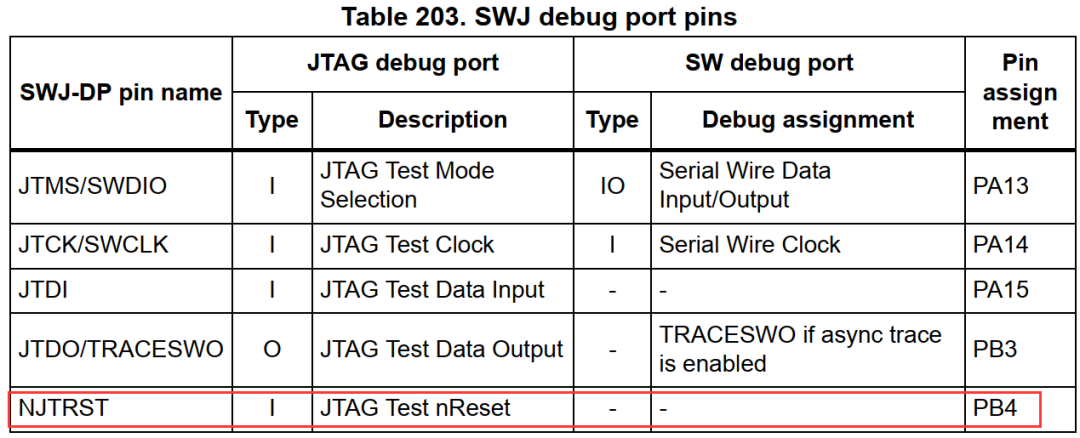
The TRST pin defined in JTAG is used to reset the TAP controller. In the STM32 series microcontrollers, there is no TRST pin; it is called NJTRST.
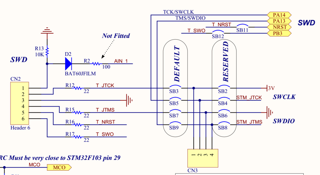
Taking STM32F207 as an example, the NJTRST pin description in JTAG and SWD modes.
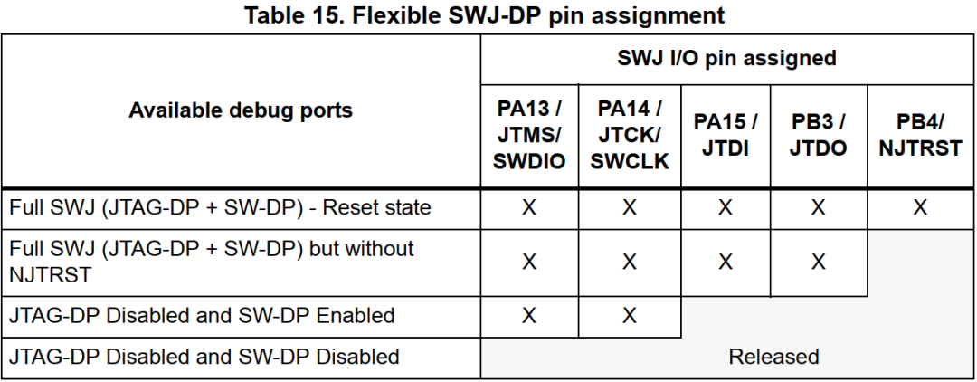
The SWJ I/O pin availability of STM32F207
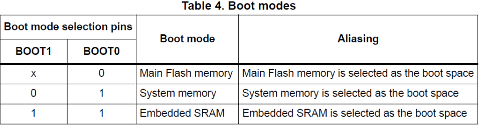
When simulating some STM32 products using 4 line SWD mode, the release version usually sets the JTAG port as a normal IO, or due to insufficient pins, is used for other purposes in the release version. When debugging the release version, since the JTAG mode is disabled, emulation is not possible.
At this time, the most common practice is to pull up the BOOT0 pin to enter the Main Flash memory mode for debugging emulation.
Comparing with the official development board of STM32, we find that using SWD mode without pulling out the RST pin is common. Of course, the SWD also includes the SWO signal, which is used for monitoring and is very useful. Both signals can be connected to the emulator.
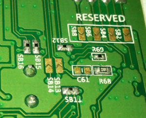
On the board for comparison:
The emulator has an Under Reset mode, so when the emulator needs to perform emulation, it sends the RST signal to the MCU, keeping the MCU in RST, or uses the Reset after emulation, where the code has not yet executed to the disabled JTAG state, allowing direct emulation. Of course, it is also possible to actively reset the power supply, which can also exit the original JTAG disabled state. You can also pull up the boot0 pin.

ScanFPGA Home
FPGA Home

Welcome FPGA, Embedded, Signal Processing engineers to follow the public account
Follow MeTech Heroes!

The Largest FPGA Technical Group Community in the Country

Welcome everyone to join the largest and strongest FPGA WeChat technical group. This group has tens of thousands of engineers, a group of engineers who love technology, and here FPGA engineers help each other, share knowledge, and have a strong technical atmosphere! Hurry up and invite your friends to join!

Just press and hold to join the national FPGA technical group!

One of the best Xilinx and Altera chip suppliers in the country!
Platform self-operated, imported original quality guarantee!
Continuously supplying multiple military research institutes and listed companies!
The best FPGA chip prices and the best after-sales service!
With the industry’s top service reputation!
Global top supplier quality standard endorsement!
Full range of XILINX orders or stock advantages!
XCVU9P-2FLGB2104I 200PCS
XCVU9P-2FLGA2104I 500PCS
XCVU13P-2FLGB2104I 300PCS
XC7K325T-2FFG900I 1500PCS
XC7K325T-2FFG676I 950PCS
XC7K160T-2FFG676I 850PCS
XC7VX690T-2FFG1927I Coming soon, please reserve!
XC7VX690T-2FFG1761I Coming soon, please reserve!
For more Xilinx model requirements, please consult us! Thank you! Scan the QR code to get in touch!

Official thanks to the brands supporting the FPGA technical group: Xilinx, Intel (Altera), Microsemi (Actel), Lattice, Vantis, Quicklogic, Lucent, etc. for their support to the technical group!