JTAG is an IEEE standard (1149.1) developed in the 1980s to address manufacturing issues in electronic boards. Today, it can be used for programming, debugging, and probing ports. But first, let’s look at JTAG’s original purpose: boundary testing.
Boundary Testing
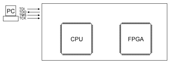
This is a simple electronic board (also known as a “Printed Circuit Board” or “PCB”) with two ICs (“Integrated Circuits”), one CPU, and one FPGA. A typical circuit board may have more ICs.
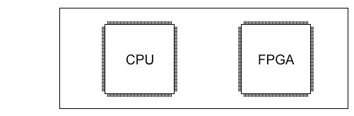
ICs can have many pins. Therefore, ICs are connected together through numerous connections (PCB traces). Only four are shown here. However, thousands can easily be placed on a PCB.
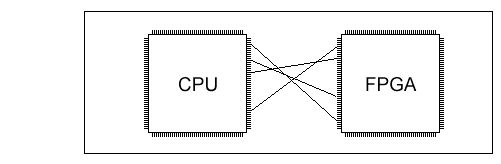
Now, if you build a thousand boards, each with thousands of connections, there will inevitably be some bad boards. How do you test all these boards? You must ensure that all these connections are correct. You cannot just manually test all these connections. This is where JTAG was created.
JTAG can control (or hijack) all IC pins. In the image, perhaps JTAG will make all CPU pins output and all FPGA pins input. Then, by sending some data from the CPU pins and reading values from the FPGA pins, JTAG can ensure that the circuit board is well-connected.
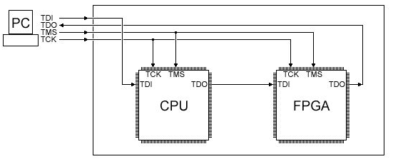
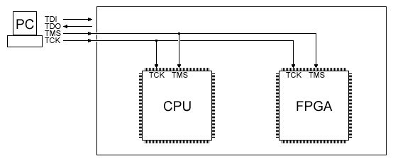
Now, JTAG actually consists of four logic signals: TDI, TDO, TMS, and TCK. From the perspective of the PC, this is three outputs and one input.
◇TCK: Clock signal, providing an independent, basic clock signal for TAP operations.
◇TMS: Mode select signal, used to control the transitions of the TAP state machine.
◇TDI: Data input signal.
◇TDO: Data output signal.
These four signals need to be wired in a specific way. First, TMS and TCK are connected in parallel with all JTAG ICs.
Then connect TDI and TDO together to form a chain. In JTAG terminology, you often hear about the term “JTAG-chain”.
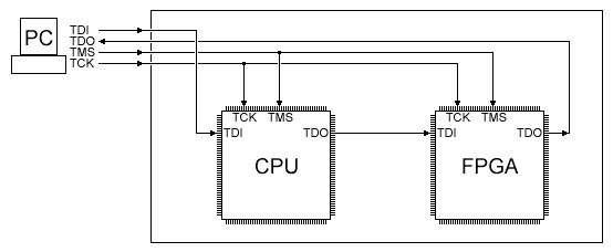
As you can see, each JTAG-compliant IC has four pins for JTAG (three inputs and one output). A fifth pin called TRST is optional (JTAG reset). JTAG pins are usually dedicated (not shared for other purposes).
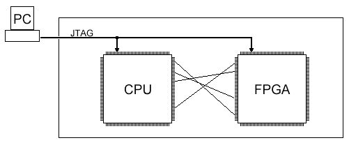
All large ICs use boundary testing done through JTAG—boundary testing is the original reason for creating JTAG. Today, the use of JTAG has expanded to allow operations such as configuring FPGAs and then debugging inside the FPGA core using JTAG.
Recommended Albums
1. FPGA Digital Image Processing
2. FPGA Digital Signal Processing
3. FPGA Learning Notes
4. ZYNQ Learning Notes
5. Vivado Learning Notes
For more exciting recommendations, please follow us

This article is sourced from: https://www.fpga4fun.com/JTAG1.html