
He is the “Little Horse” mentioned by TK at the GeekPwn conference in 2015, another alchemist who intruded into the security circle (originally a chemistry major) – HyperChem. After a few years of experience in software unpacking, he is currently focusing on embedded security and firmware reverse engineering.
This researcher from Tencent Security’s Xuanwu Lab, HyperChem, shared insights in the field of smart hardware security at the GeekPwn2017 Shanghai “Geek Salon”.
“JTAG debugging has extraordinary power for embedded security research; it can read and write memory, control CPU operation states, and debug code, almost nothing is impossible. But how do you perform JTAG debugging on an unknown device? What steps and preparations are needed for JTAG debugging? This theme will reveal everything one by one.”
Hello everyone, I am HyperChem from Tencent Security’s Xuanwu Lab, you can also call me HC. Today I will share about JTAG debugging; those engaged in embedded security may be familiar with JTAG, and if we can obtain debugging permissions, it will be very useful for us.
What Exactly Is JTAG?
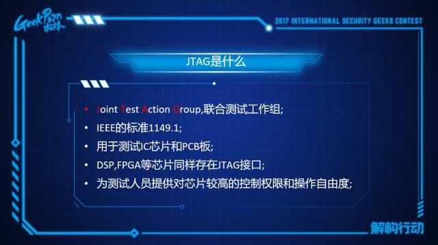
JTAG is actually an abbreviation for Joint Test Action Group, which later became a standard, specifically IEEE standard 1149.1. Initially, JTAG was used to test whether IC chips could operate normally; DSP, FPGA, and other chips also have JTAG.
JTAG can debug chips and control them to execute any code. During embedded development, it is used to download firmware; if you have played with routers, you should have programmed using JTAG, and of course, we can also use JTAG to read and write memory.
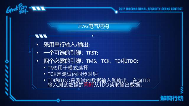
Let’s first understand the electrical structure of JTAG. It has an optional pin TRST and four mandatory pins: TMS, TCK, TDI, and TDO. JTAG is actually controlled through the Test Access Port, and the JTAG controller has 16 states. The state transitions are accomplished by the JTAG TMS pin toggling between 1 and 0.
JTAG commands. It specifies several mandatory commands in 1149.1, one being the bypass command to speed up testing, and another external test instruction used to enable testing of external circuits. There are also internal test instructions for testing components like internal buses within the chip. Additionally, most IC chips have an IDCODE, which typically corresponds to an IDCODE command.
For Example: A Simple JTAG
We output from these 6 pins and set up 6 shift registers. When you are not performing JTAG debugging, these 6 shift registers are useless, but when we perform JTAG debugging, we write values to the real pins through these shift registers and can also read the current pin states through the shift registers. This is because JTAG was initially designed to monitor the states of the chip’s input/output pins, which are located on the boundaries of the chip, hence the term boundary scan chain.
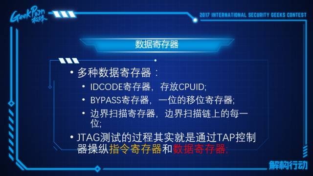
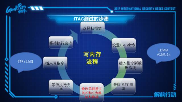
JTAG has about 3 registers: one is the IDCODE register, another is the BYPASS register, and the boundary scan register. The JTAG testing process is actually completed through the TAP. So, how does JTAG achieve such an attempt? Let’s take the memory writing process of an ARMV9 chip as an example.
First, we need to select a boundary scan chain, control the data inside, and then set a JTAG command, which is to select the internal test mode, meaning an internal test command that will cause all operations to occur inside the CPU, and our reads and writes will not affect the contents of memory and external devices.
As we know, when the CPU executes instructions, there is a phase where it reads the instruction onto the data bus; at this point, we write an instruction to the data bus that means to write R0 and R1 to the address pointed to by R0. However, the significance of this instruction is not important; the key operation is that the values of R0 and R1 will appear in the subsequent execution phase. In the next execution phase, we will modify the data bus to change the values of R0 and R1 to what we need.

Once it completes execution, this operation will not cause any impact. Next, we adjust the execution mode of the next instruction, setting a flag that can temporarily hang in internal test mode, meaning this instruction will actually perform operations and will truly write data. Then we wait for the execution to complete, and the entire memory writing operation is complete; the memory reading process is quite similar, we just need to change STR to LDR. This is the flow of JTAG.
How to Utilize JTAG?
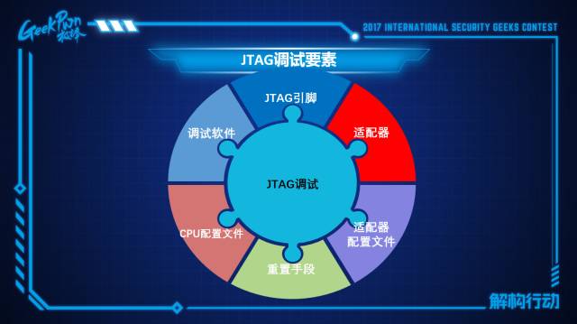
If we want to perform JTAG debugging on a device, we need to have several elements: first, we need to know where the 4 pins are so we can connect to them; then we need an adapter, which primarily completes the electrical signal conversion so that we can control the TAP controller through the computer; next, we need a configuration file for the adapter; following that, debugging software and information about the CPU to be debugged, and finally, we need a method to reset.
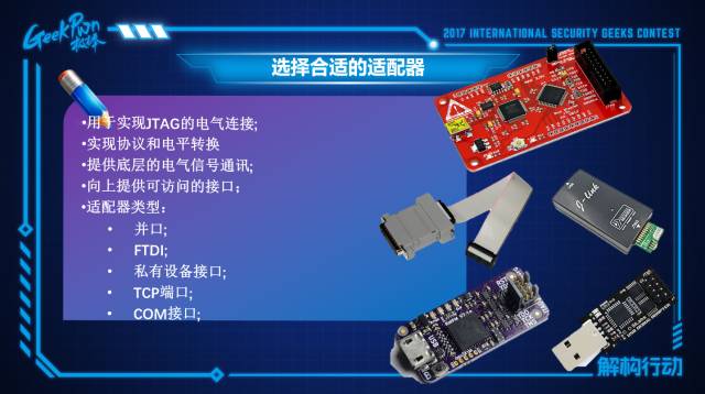
First, find the JTAG pins; currently, a good tool for finding JTAG pins is JTAGULATOR, which is an automated tool for locating JTAG pins. Next, we need a suitable adapter. I have listed some adapters above; the purpose of the adapter is primarily to achieve electrical and level conversion. As we mentioned, JTAG actually uses 1010 signals, which is quite difficult to implement through software, so we need an adapter to complete this part of the work for us.
There are several types; the earliest adapters completed debugging through the printer port. Now, the more popular adapters are of the FTDI type and some private device interfaces, as well as those using COM ports and network ports for communication. The adapter I am using for today’s demonstration is the popular FTDI interface.
Below is the debugging software. There are many software options for JTAG debugging; some software used for repairing phones are commercial, while a representative of open-source software that supports various platforms is GDB. The software we are using today is called OpenOCD, which can provide us with a good interface.
This is the CPU configuration file, which defines different CPU files in OpenOCD, including the definitions of JTAG instructions and the boundary scan chain within the CPU.
Next is the adapter configuration file, which describes how the upper-level software connects with the adapter.
Then there are reset conditions; if using commercial software, it will implement this at the electrical layer. The reset condition means that when your adapter connects to JTAG, the TAP controller and CPU can be in any state, and we do not know what its state is. We need to bring the CPU back to a known state, which requires a reset. For the CPU, there will be a pin that, when detecting too high or too low voltage, will reset it directly.
How to Perform JTAG Debugging on Unknown Devices?
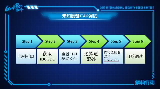
First, identify its pins, then obtain the IDCODE, and subsequently search for the CPU configuration file through the IDCODE. OpenOCD contains many CPU configuration files by default, and you can try searching among these files. Then select the appropriate adapter and its configuration file to proceed with debugging.
Reply “Geek Salon” on the GeekPwn WeChat official account to get the guest’s sharing PPT!
Selected Highlights from Previous Issues

Highlights from GeekPwn2017 Shanghai Station
Highlights from GeekPwn2017 Silicon Valley Station
Hacker vs AI Security Challenge


GeekPwn2018 Contestant Recruitment Has Started
Long press the QR code to follow!