Author: Hcamael@Zhidao Chuangyu 404 Laboratory Date: October 21, 2019
Recently, while working on a router, I accidentally bricked the CFE and discovered that I could recover it through JTAG, so I did some research on JTAG.
Initially, I only wanted to recover the brick, without any intention of deep research.
Brick Recovery Attempt
The bricked router model is: LinkSys WRT54G v8
CPU model: BCM5354
Flash model: K8D6316UBM
First, I obtained the order of the JTAG interface on the device using JTAGulator.
Fortunately, the company had a J-Link, but my attempts failed as it couldn’t recognize the device.
I later found a tool called: tjtag-pi[1] through Google, which can control JTAG using Raspberry Pi, so I learned how to operate the Raspberry Pi.
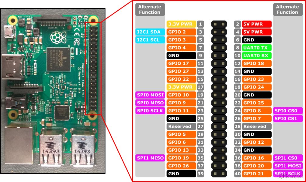
Raspberry Pi Pins
I used an RPi3, and the pinout diagram is as follows:
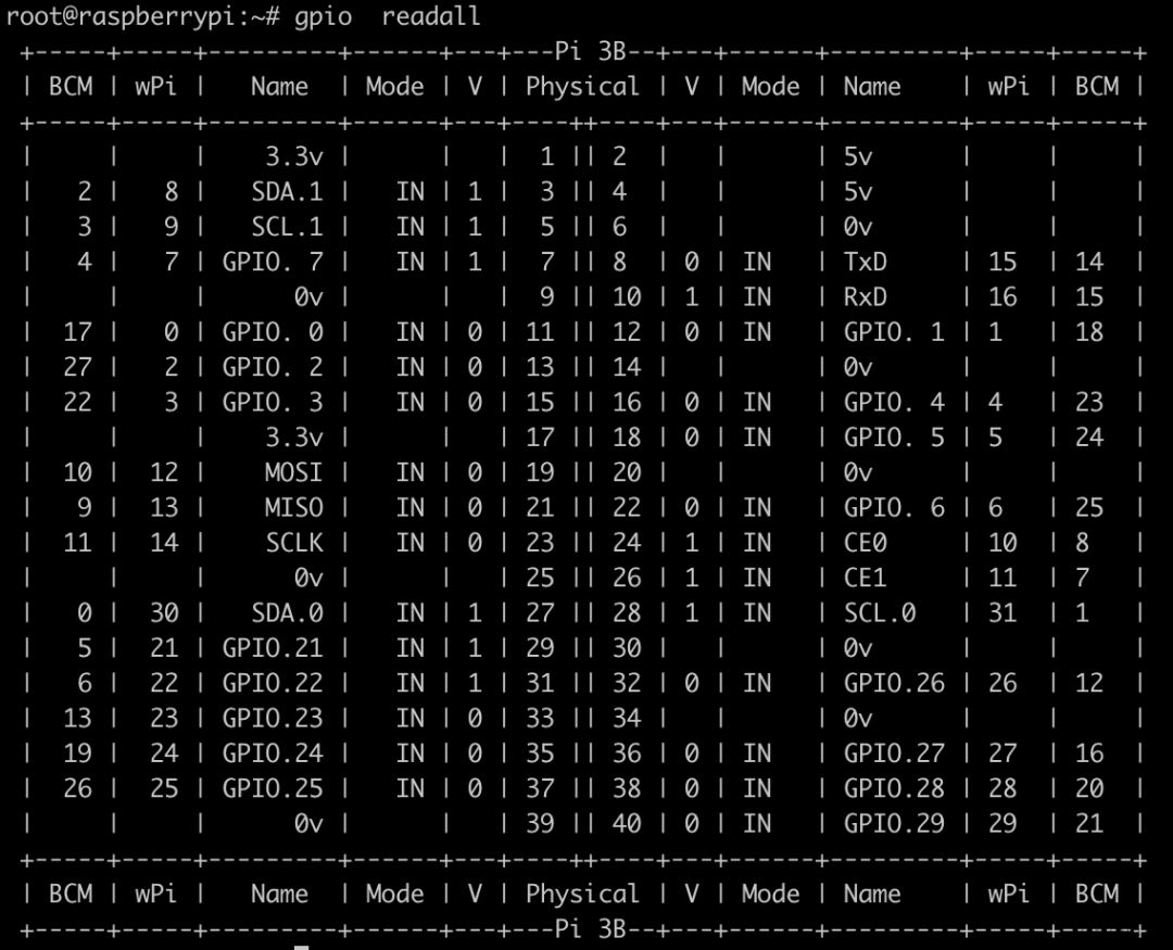
Or you can use gpio readall on Raspberry Pi 3 to check the status of each pin:
The RPi3 has a RPi.GPIO module in Python that can control these pins.
For example:
>>> from RPi import GPIO
>>> GPIO.setmode(GPIO.BCM)
>>> GPIO.setup(2, GPIO.OUT)
>>> GPIO.setup(3, GPIO.IN)
First, you need to initialize the GPIO mode; the BCM mode corresponds to the pin arrangement in the orange section of the diagram above.
Then you can set each pin individually, for example, in the diagram above, set pin 2 as output and pin 3 as input.
>>> GPIO.output(2, 1)
>>> GPIO.output(2, 0)
Use the output function for binary output.
>>> GPIO.input(3)1Use the input function to get the input of the pin.
We can connect the two pins with a wire to test the above code.
After connecting the Raspberry Pi corresponding pins to the router, you can run the tjtag-pi program. However, during the process, I encountered issues, often getting stuck while writing to flash. By adjusting the configuration, it sometimes succeeded, but the CFE was not recovered, and backing up the flash data showed that the data was not successfully written.
Since using the existing tool failed, I had to try to research and create my own solution.
JTAG
First, regarding the pins, devices I have seen typically provide more than 5 * 2 pins for JTAG. Among these, there are usually grounding pins, and the other half only needs to know the four most important pins.
The order of these four pins is generally as follows:
TDI TDO TMS TCKTDI represents input, TDO represents output, TMS is the control bit, and TCK is the clock input.
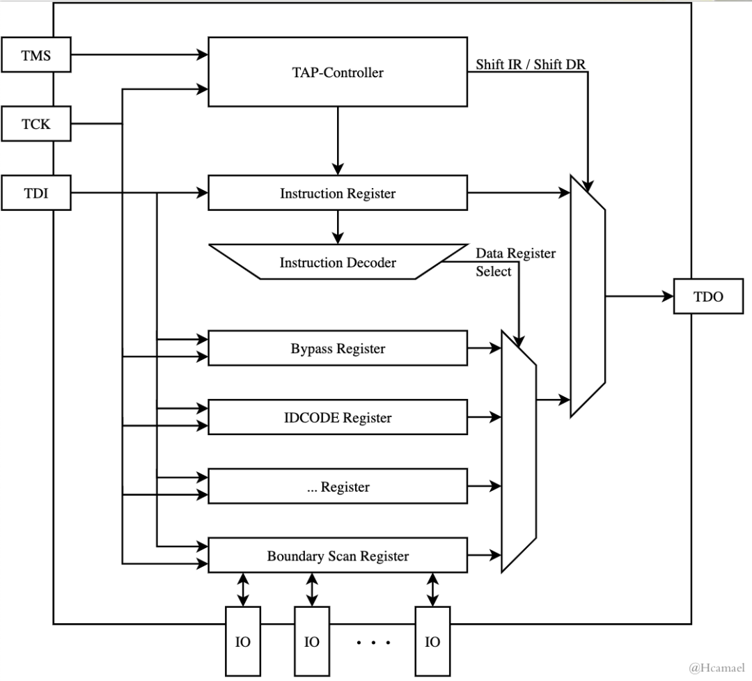
The general architecture of JTAG is illustrated in the above image, and the architecture of the TAP-Controller is shown in the following image:
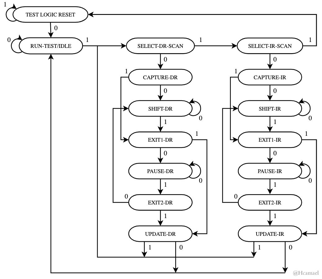
Based on the above two architectures, I will explain the principles of JTAG.
The core of JTAG is the TAP-Controller, which determines the relationship between input and output by parsing TMS data. So let’s first take a look at the architecture of the TAP-Controller.
From the above diagram, we can see that in any state, outputting five 1’s will return to the TEST LOGIC RESET state. Therefore, before using JTAG, we first send five 1’s through the TMS port; the JTAG state machine will enter the RESET recovery state.
When the TAP enters the SHIFT-IR state, the Instruction Register will start receiving data from TDI. After the input ends, when it enters the UPDATE-IR state, it will parse the value of the instruction register and then decide what data to output.
SHIFT-DR controls the data register, which is generally used when reading and writing data.
At this point, a question arises: TMS has only one port, how does JTAG know the value of TMS input each time? This is where the TCK port comes into play, which can be termed as the clock instruction. When TCK transitions from low frequency to high frequency, it captures one bit of TMS/TDI input, and TDO outputs one bit.
For example, to perform a reset operation with TAP:
for x in range(5):
    TCK 0
    TMS 1
    TCK 1
For example, to input 0b10 to the instruction register:
1. Reset
2. Enter RUN-TEST/IDLE state
TCK 0
TMS 0
TCK 1
3. Enter SELECT-DR-SCAN state
TCK 0
TMS 1
TCK 1
4. Enter SELECT-IR-SCAN state
TCK 0
TMS 1
TCK 1
5. Enter CAPTURE-IR state
TCK 0
TMS 0
TCK 1
6. Enter SHIFT-IR state
TCK 0
TMS 0
TCK 1
7. Input 0b10
TCK 0
TMS 0
TDI 0
TCK 1
TCK 0
TMS 1
TDI 1
TCK 0
Then we enter EXIT-IR -> UPDATE-IR.
Based on the theory above, we can write a function to set the IR:
def clock(tms, tdi):
    tms = 1 if tms else 0
    tdi = 1 if tdi else 0
    GPIO.output(TCK, 0)
    GPIO.output(TMS, tms)
    GPIO.output(TDI, tdi)
    GPIO.output(TCK, 1)
    return GPIO.input(TDO)
def reset():
    clock(1, 0)
    clock(1, 0)
    clock(1, 0)
    clock(1, 0)
    clock(1, 0)
    clock(0, 0)
def set_instr(instr):
    clock(1, 0)
    clock(1, 0)
    clock(0, 0)
    clock(0, 0)
    for i in range(INSTR_LENGTH):
        clock(i==(INSTR_LENGTH - 1), (instr>>i)&1)
    clock(1, 0)
    clock(0, 0)
Understanding the above code basically leads to a comprehension of TAP logic. Next comes the instruction issue: what is the length of the instruction register? What values are meaningful for the instruction register?
Different CPUs have different answers to the above questions. From my online searches, it seems that each CPU should have a boundary scan description (BSD) file. The CPU model studied in this article is BCM5354, but I couldn’t find the BSD file for this model online. I could only refer to a BSD file of a different model from the same manufacturer.
bcm53101m.bsd[2]
In this file, we can see the position of the JTAG port on the CPU port:
"tck              : B46  , " & "tdi              : A57  , " & "tdo              : B47  , " & "tms              : A58  , " & "trst_b           : A59  , " &

attribute TAP_SCAN_RESET of trst_b                   : signal is true;attribute TAP_SCAN_IN    of tdi                      : signal is true;attribute TAP_SCAN_MODE  of tms                      : signal is true;attribute TAP_SCAN_OUT   of tdo                      : signal is true;attribute TAP_SCAN_CLOCK of tck                      : signal is (2.5000000000000000000e+07, BOTH);
We can find the definition of instruction length:
attribute INSTRUCTION_LENGTH of top: entity is 32;We can find the valid values for the instruction register:
attribute INSTRUCTION_OPCODE of top: entity is "IDCODE (11111111111111111111111111111110)," & "BYPASS (00000000000000000000000000000000, 11111111111111111111111111111111)," & "EXTEST (11111111111111111111111111101000)," & "SAMPLE (11111111111111111111111111111000)," & "PRELOAD (11111111111111111111111111111000)," & "HIGHZ (11111111111111111111111111001111)," & "CLAMP (11111111111111111111111111101111) " ;When the value of the instruction register is IDCODE, the output channel of the IDCODE register is enabled. Let’s take a look at the IDCODE register:
attribute IDCODE_REGISTER of top: entity is "0000" & -- version "0000000011011111" & -- part number "00101111111" & -- manufacturer's identity "1"; -- required by 1149.1From here we can see that the fixed output of the IDCODE register is: 0b00000000000011011111001011111111
So how do we obtain the TDO output? This is when the data register (DR) comes into play.
1. The TAP state machine switches to SHIFT-IR2. Output IDCODE to IR3. Switch to SHIFT-DR4. Obtain TDO output value with a length of INSTRUCTION_LENGTH5. Exit
Representing this in code form:
def ReadWriteData(data):
    out_data = 0
    clock(1, 0)
    clock(0, 0)
    clock(0, 0)
    for i in range(32):
        out_bit  = clock((i == 31), ((data >> i) & 1))
        out_data = out_data | (out_bit << i)
    clock(1,0)
    clock(0,0)
    return out_data
def ReadData():
    return ReadWriteData(0)
def WriteData(data):
    ReadWriteData(data)
def idcode():
    set_instr(INSTR_IDCODE)
    print(hex(self.ReadData()))
As I am also a beginner, I cannot fully understand the content in the boundary scan description file; for example, it is unclear what the BYPASS instruction does. However, I learned from other documents that the BYPASS register is generally used for testing, where the input and output are directly connected, allowing comparison of input and output values to determine if the port is correctly connected.
Additionally, there is a lot of data related to the boundary scan register, which I have not fully researched, and there is scarce related information. Moreover, I cannot find the corresponding CPU documentation.
At this point in my research, I only understood the basic principles of JTAG and could only use two basic instructions (IDCODE, BYPASS). However, this was not helpful in recovering the brick.
Left with no choice, I went back to look at the source code of tjtag, which defines several instruction register OPCODES:
INSTR_ADDRESS = 0x08
INSTR_DATA    = 0x09
INSTR_CONTROL = 0x0A
By copying the flash operations for AMD in tjtag, I could successfully perform erase, write, and read operations on flash, but I did not understand the principles behind it.
Here I will share my script: jtag.py[3]
Flash documentation: https://www.dataman.com/media/datasheet/Samsung/K8D6x16UTM_K8D6x16UBM_rev16.pdf
Next, I will study this flash documentation and share my subsequent research results in future articles.

Past Popular Articles
(Click the image to jump)


If you think it’s good, please click ‘Looking’!