01
JTAG (Joint Test Action Group) is an international standard testing protocol (IEEE 1149.1 compliant) primarily used for internal chip testing. Most advanced devices now support the JTAG protocol, such as DSPs and FPGAs. The standard JTAG interface consists of four lines: TMS (Test Mode Select), TCK (Test Clock Input), TDI (Test Data Input), and TDO (Test Data Output). JTAG was originally designed for testing chips, and its basic principle is to define a TAP (Test Access Port) within the device to test internal nodes using specialized JTAG testing tools. JTAG testing allows multiple devices to be connected in series through the JTAG interface, forming a JTAG chain, enabling separate testing of each device. Nowadays, the JTAG interface is also commonly used for implementing ISP (In-System Programming) to program devices like FLASH.
02
When a system contains multiple (more than two) Xilinx FPGAs, CPLDs, or PROMs (FLASH) with the same level, we do not need to bring out the JTAG for each IC. Instead, we can use a single JTAG port to connect all chips in a daisy chain configuration, as shown in the figure below.
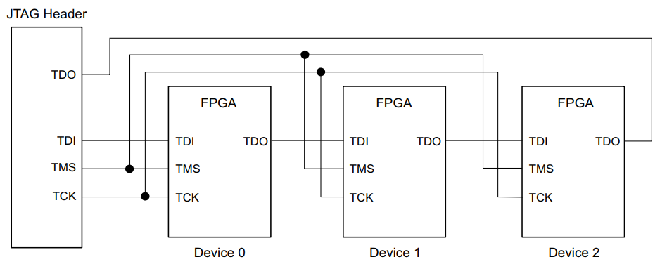
This approach has two benefits: (1) it saves PCB space occupied by multiple JTAG ports, which is particularly suitable for space-constrained embedded systems, such as small industrial cameras; (2) embedded systems often operate in closed environments, and sometimes require online or remote upgrades of the FPGA programs, necessitating the JTAG port to be accessible from outside the chassis. Clearly, this single JTAG port daisy chain structure is the best choice.
03
Since the TCK and TMS signals are connected to all chips in the daisy chain, the quality (integrity) of these two signals is very important! Especially for the clock signal TCK, any glitches or edge jitter can lead to download failures.
When there are more than three chips (or devices) in the daisy chain, TMS and TCK must be buffered (e.g., using 74LVC245) to increase their driving capability, which is particularly important for some domestic programmers with poor driving capabilities. The number of chips (or devices) in each branch link where the driver gate is located depends on the driving capability of the buffer. Generally, one buffer gate of 74LVC245 (8 buffers) can drive 3 to 4 loads (chips). A resistor of 20 to 30Ω should be connected in series at the output of the TCK buffer, and a capacitor of 100 to 1000pF should be connected to ground at the device end to significantly reduce edge jitter and minimize glitch interference.
TMS is a mode select switch signal, and TCK is a clock pulse signal with a default frequency of 6MHz. When the load is heavier, reducing the TCK frequency without buffering can also improve signal integrity.
The JTAG protocol specifies that the TDI data is valid on the falling edge of TCK, and the TDO data is sampled on the rising edge of TCK. Therefore, it is essential to ensure that the propagation delay (TCPD) from TDI to TDO across the entire JTAG chain must be less than half of the TCK period (TCLK/2), i.e., △T = TCLK/2 – TCPD > 0. This means that with increased buffering, the total number of chips in the JTAG chain is related to the TDO delay (TDOV) of each chip (FPGA is TTCKTDO) and the TCK frequency. After determining the total number of chips, to ensure △T > 0, the TCK frequency can be reduced.
04
Note:
The topology of JTAG is quite peculiar, even though the frequency is not high. TMS and TCK are in a parallel structure with one master and multiple slaves; TDI and TDO are in a series structure with one master and one slave. If there are no buffers for TMS and TCK on the board, and the layout and routing are not good enough, there will be significant overshoot on TCK. As long as an overshoot causes an erroneous edge, JTAG will fail. The solution is to lower the TCK frequency, add small resistors in series, and connect small capacitors at the TCK/TMS terminals.