Skip to content
 Flash is a type of non-volatile memory that can retain data even when power is off. It is a form of electronically erasable programmable read-only memory (EEPROM) that allows for multiple erase and write cycles during operation. This technology is primarily used for general data storage and for transferring data between computers and other digital products, such as storage cards and flash drives.
The current development status of Flash chip technology: (1) With the widespread application of solid-state storage, Flash has rapidly developed, and chip manufacturing processes have continuously improved; (2) Meanwhile, the structure of NAND-type Flash cells has also changed significantly, evolving from the initial single-level cell (SLC) structure that stores one bit per cell to multi-level cells (MLC, TLC, etc.) that can store multiple bits per cell, with single-chip capacities continually increasing; (3) After long-term technological accumulation, Samsung launched its 3D NAND Flash technology in 2013, and companies like Toshiba, Micron, and SK Hynix announced their timelines for 3D NAND Flash sample delivery and mass production. The 3D NAND technology is fundamentally different from existing 2D NAND technology; simply put, 2D NAND has a planar structure while 3D NAND has a three-dimensional structure. The 3D technology not only improves product performance by at least 20% but also reduces power consumption by over 40%; (4) Solid-state drives are gradually replacing mechanical hard drives; (5) In enterprise applications, Flash is used as a hardware acceleration card to construct integrated storage systems; (6) For enterprise applications that require high concurrency and low latency, a working group led by Intel released the NVMe (Non-volatile Memory Express) protocol standard in 2010, which defines a register interface and command set specifically for non-volatile memory subsystems.
Based on industry development needs, the high-end storage system research group of the State Intellectual Property Office’s patent analysis promotion project has conducted an in-depth analysis of Flash technology from five perspectives: programming interference resistance, 3D Flash technology, the Flash alliance between Toshiba and SanDisk, Flash industry litigation, and the Flash industry patent pool.
PART 1 Programming Interference Resistance
Flash is a type of non-volatile memory that can retain data even when power is off. It is a form of electronically erasable programmable read-only memory (EEPROM) that allows for multiple erase and write cycles during operation. This technology is primarily used for general data storage and for transferring data between computers and other digital products, such as storage cards and flash drives.
The current development status of Flash chip technology: (1) With the widespread application of solid-state storage, Flash has rapidly developed, and chip manufacturing processes have continuously improved; (2) Meanwhile, the structure of NAND-type Flash cells has also changed significantly, evolving from the initial single-level cell (SLC) structure that stores one bit per cell to multi-level cells (MLC, TLC, etc.) that can store multiple bits per cell, with single-chip capacities continually increasing; (3) After long-term technological accumulation, Samsung launched its 3D NAND Flash technology in 2013, and companies like Toshiba, Micron, and SK Hynix announced their timelines for 3D NAND Flash sample delivery and mass production. The 3D NAND technology is fundamentally different from existing 2D NAND technology; simply put, 2D NAND has a planar structure while 3D NAND has a three-dimensional structure. The 3D technology not only improves product performance by at least 20% but also reduces power consumption by over 40%; (4) Solid-state drives are gradually replacing mechanical hard drives; (5) In enterprise applications, Flash is used as a hardware acceleration card to construct integrated storage systems; (6) For enterprise applications that require high concurrency and low latency, a working group led by Intel released the NVMe (Non-volatile Memory Express) protocol standard in 2010, which defines a register interface and command set specifically for non-volatile memory subsystems.
Based on industry development needs, the high-end storage system research group of the State Intellectual Property Office’s patent analysis promotion project has conducted an in-depth analysis of Flash technology from five perspectives: programming interference resistance, 3D Flash technology, the Flash alliance between Toshiba and SanDisk, Flash industry litigation, and the Flash industry patent pool.
PART 1 Programming Interference Resistance
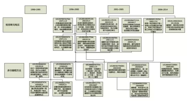 From a temporal perspective, the technological improvements in programming interference resistance regarding adjacent cell voltages and multi-programming methods have primarily gone through three stages: the initial passive repair of interference through detection (e.g., US19970974276A and US19920886030A), followed by the active suppression of interference through applying different voltages (e.g., US20010039518A, US20020112923A, and KR19950030747A), and finally through a combination of detection and active adjustment to reduce interference (e.g., US20040765693A and US20090572098A), evolving from a broad treatment to fine-tuning, and then to comprehensive processing (a combination of treating the symptoms and the root cause).
In terms of technical effects, the early period (1990-1995) mainly focused on how to eliminate the cumulative interference issues between adjacent strings, which was more evident in the multi-programming section. Subsequently (1996-2000), major companies became more precise in their focus, paying attention to interference between adjacent cells, such as the Yupin effect. From 2001 to 2014, the focus shifted to both interference between adjacent strings and between adjacent cells. Notably, SanDisk accounted for nearly half of the important patents, highlighting its strong capabilities, followed closely by Samsung and Toshiba.
PART 2 3D Flash Technology
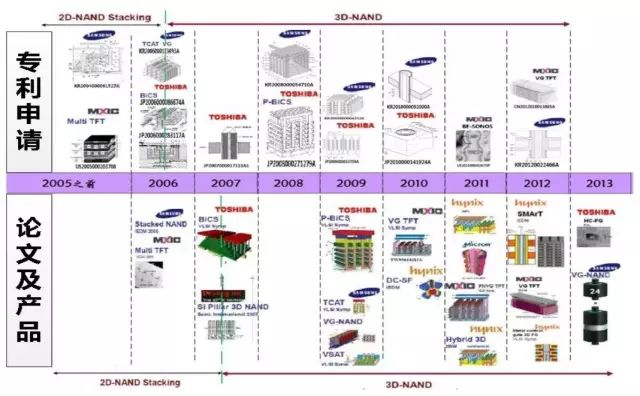
Before 2005: Simple stacking structure: maintaining the bit line and word line in the same plane, with the layers of memory stacked vertically one on top of the other, referred to as simple stacking. Before 2006 (including 2006), there were very few reports on 3D NAND technology, with only Samsung and Winbond presenting at international conferences, showcasing a two-layer memory stack, with Samsung using the SEG structure and Winbond opting for the TFT structure.
In 2006, Toshiba filed a patent application for 3D Flash (application number: JP2006000086674, application date: 20060327) and presented the industry-shaking 3D NAND structure known as BiCS (bit cost scalable) at the VLSI international conference in 2007.
Inspired by Toshiba’s 3D Flash structure, other flash memory companies quickly proposed their own 3D Flash structures, and by 2014, various companies’ 3D Flash products began to hit the market.
From a temporal perspective, the technological improvements in programming interference resistance regarding adjacent cell voltages and multi-programming methods have primarily gone through three stages: the initial passive repair of interference through detection (e.g., US19970974276A and US19920886030A), followed by the active suppression of interference through applying different voltages (e.g., US20010039518A, US20020112923A, and KR19950030747A), and finally through a combination of detection and active adjustment to reduce interference (e.g., US20040765693A and US20090572098A), evolving from a broad treatment to fine-tuning, and then to comprehensive processing (a combination of treating the symptoms and the root cause).
In terms of technical effects, the early period (1990-1995) mainly focused on how to eliminate the cumulative interference issues between adjacent strings, which was more evident in the multi-programming section. Subsequently (1996-2000), major companies became more precise in their focus, paying attention to interference between adjacent cells, such as the Yupin effect. From 2001 to 2014, the focus shifted to both interference between adjacent strings and between adjacent cells. Notably, SanDisk accounted for nearly half of the important patents, highlighting its strong capabilities, followed closely by Samsung and Toshiba.
PART 2 3D Flash Technology
Before 2005: Simple stacking structure: maintaining the bit line and word line in the same plane, with the layers of memory stacked vertically one on top of the other, referred to as simple stacking. Before 2006 (including 2006), there were very few reports on 3D NAND technology, with only Samsung and Winbond presenting at international conferences, showcasing a two-layer memory stack, with Samsung using the SEG structure and Winbond opting for the TFT structure.
In 2006, Toshiba filed a patent application for 3D Flash (application number: JP2006000086674, application date: 20060327) and presented the industry-shaking 3D NAND structure known as BiCS (bit cost scalable) at the VLSI international conference in 2007.
Inspired by Toshiba’s 3D Flash structure, other flash memory companies quickly proposed their own 3D Flash structures, and by 2014, various companies’ 3D Flash products began to hit the market.
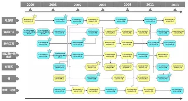
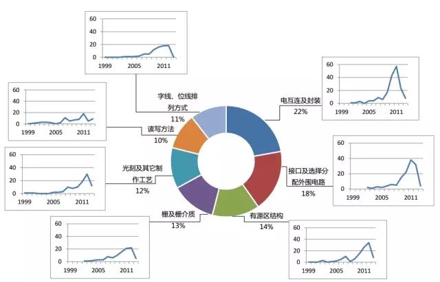 Typically, the research and development of multiple technical branches of key technologies occur in a sequential manner. From the diagram, we can see that 3D Flash has seven technical branches, namely word line and bit line arrangements, electrical interconnections and packaging, interface and selection distribution of peripheral circuits, read/write methods, photolithography and other manufacturing processes, gate and gate dielectric, and active region structure. The development of each technical branch is balanced, and the application trends are consistent, indicating that 3D technology is the trend in the Flash industry.
Overall, Chinese companies have a very limited number of patent applications in the field of 3D Flash technology, and there is a significant gap in patent layout compared to leading companies like Samsung and Toshiba, indicating considerable room for improvement.
PART 3 The Flash Alliance Between Toshiba and SanDisk
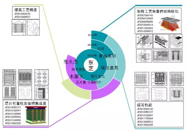
Toshiba’s inventor team, led by Akira Yoshida, has been leading various R&D teams to achieve corresponding patent layouts in various technical fields of 3D Flash since 2006. This mainly involves process precision, structural optimization, chip reliability, and read/write performance.
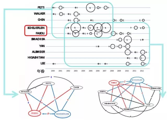
Since 2002, SCHEUERLEIN R E and FASOLI L from SanDisk’s 3D Flash R&D team have applied for patents. SCHEUERLEIN R E and FASOLI L closely collaborated with key applicants PETTI C J, WALKER A J, and COSTA in the early technical R&D of SanDisk’s 3D Flash, applying for a series of patents mainly related to read/write methods, interfaces, and peripheral circuits.
Toshiba and SanDisk not only have excellent R&D teams but also closely collaborate in their research and development. The yellow section in the diagram represents Toshiba’s patent applications, while the blue section represents SanDisk’s, with the starred items indicating key patent applications.
From the diagram, it can be seen that Toshiba and SanDisk’s patent applications are integrated, with each company improving and refining the patent applications under the same technical branches, forming a complete technological roadmap together.
PART 4 Flash Industry Litigation
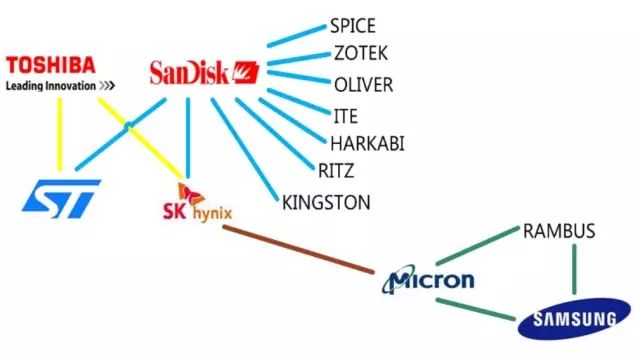
The flash memory market has developed over 30 years, with an annual output value exceeding $30 billion, making it a significant market. Companies from the US, Japan, and South Korea started early, have strong technological capabilities, and place great importance on protecting intellectual property, leading to a series of patent litigation events among major manufacturers, resulting in a competitive landscape. The focus remains on Toshiba and SanDisk for studying patent litigation in this industry.
SanDisk and Toshiba have jointly litigated against several companies. Samsung, Micron, and Rambus have been involved in litigation, but there has been no direct confrontation between Samsung and the SanDisk-Toshiba alliance.
Typically, the research and development of multiple technical branches of key technologies occur in a sequential manner. From the diagram, we can see that 3D Flash has seven technical branches, namely word line and bit line arrangements, electrical interconnections and packaging, interface and selection distribution of peripheral circuits, read/write methods, photolithography and other manufacturing processes, gate and gate dielectric, and active region structure. The development of each technical branch is balanced, and the application trends are consistent, indicating that 3D technology is the trend in the Flash industry.
Overall, Chinese companies have a very limited number of patent applications in the field of 3D Flash technology, and there is a significant gap in patent layout compared to leading companies like Samsung and Toshiba, indicating considerable room for improvement.
PART 3 The Flash Alliance Between Toshiba and SanDisk
Toshiba’s inventor team, led by Akira Yoshida, has been leading various R&D teams to achieve corresponding patent layouts in various technical fields of 3D Flash since 2006. This mainly involves process precision, structural optimization, chip reliability, and read/write performance.
Since 2002, SCHEUERLEIN R E and FASOLI L from SanDisk’s 3D Flash R&D team have applied for patents. SCHEUERLEIN R E and FASOLI L closely collaborated with key applicants PETTI C J, WALKER A J, and COSTA in the early technical R&D of SanDisk’s 3D Flash, applying for a series of patents mainly related to read/write methods, interfaces, and peripheral circuits.
Toshiba and SanDisk not only have excellent R&D teams but also closely collaborate in their research and development. The yellow section in the diagram represents Toshiba’s patent applications, while the blue section represents SanDisk’s, with the starred items indicating key patent applications.
From the diagram, it can be seen that Toshiba and SanDisk’s patent applications are integrated, with each company improving and refining the patent applications under the same technical branches, forming a complete technological roadmap together.
PART 4 Flash Industry Litigation
The flash memory market has developed over 30 years, with an annual output value exceeding $30 billion, making it a significant market. Companies from the US, Japan, and South Korea started early, have strong technological capabilities, and place great importance on protecting intellectual property, leading to a series of patent litigation events among major manufacturers, resulting in a competitive landscape. The focus remains on Toshiba and SanDisk for studying patent litigation in this industry.
SanDisk and Toshiba have jointly litigated against several companies. Samsung, Micron, and Rambus have been involved in litigation, but there has been no direct confrontation between Samsung and the SanDisk-Toshiba alliance.
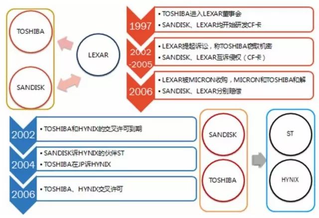 (1) In 2002, Lexar filed a lawsuit claiming that Toshiba stole its trade secrets. Both parties engaged in a prolonged legal battle. Toshiba, having balanced development across various technologies and lacking a good response strategy, relied on SanDisk to file a lawsuit against Lexar in the US for infringement of its related storage card patents. The prolonged litigation drained Lexar, ultimately leading to its acquisition by Micron, after which Toshiba and Micron reached a settlement.
(2) Toshiba and Hynix signed a cross-licensing agreement that expired, and by 2004, the two companies struggled to reach an agreement on extension fees. Toshiba filed a lawsuit against Hynix in the Tokyo court. SanDisk utilized its patent advantages to support its partner Toshiba, thus also filing a lawsuit alleging that the storage chips made by Hynix’s partner STMicroelectronics infringed SanDisk’s patents.
(3) In 2014, a new joint lawsuit was launched: after a former Toshiba employee moved to Hynix and took confidential flash memory technology documents with him, Toshiba sued Hynix in Japan, while SanDisk filed a lawsuit in the US for infringement of its trade secrets.
It can be seen that Toshiba and SanDisk, in dealing with or initiating litigation, have leveraged the power of their partners to achieve more favorable litigation outcomes, forming a litigation alliance in this case.
PART 5 Flash Industry Patent Pool
(1) In 2002, Lexar filed a lawsuit claiming that Toshiba stole its trade secrets. Both parties engaged in a prolonged legal battle. Toshiba, having balanced development across various technologies and lacking a good response strategy, relied on SanDisk to file a lawsuit against Lexar in the US for infringement of its related storage card patents. The prolonged litigation drained Lexar, ultimately leading to its acquisition by Micron, after which Toshiba and Micron reached a settlement.
(2) Toshiba and Hynix signed a cross-licensing agreement that expired, and by 2004, the two companies struggled to reach an agreement on extension fees. Toshiba filed a lawsuit against Hynix in the Tokyo court. SanDisk utilized its patent advantages to support its partner Toshiba, thus also filing a lawsuit alleging that the storage chips made by Hynix’s partner STMicroelectronics infringed SanDisk’s patents.
(3) In 2014, a new joint lawsuit was launched: after a former Toshiba employee moved to Hynix and took confidential flash memory technology documents with him, Toshiba sued Hynix in Japan, while SanDisk filed a lawsuit in the US for infringement of its trade secrets.
It can be seen that Toshiba and SanDisk, in dealing with or initiating litigation, have leveraged the power of their partners to achieve more favorable litigation outcomes, forming a litigation alliance in this case.
PART 5 Flash Industry Patent Pool
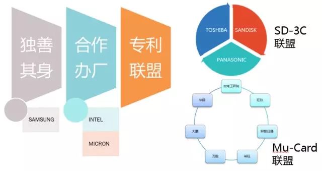 A patent pool is an effective way to manage patents by concentrating management of numerous core patents, combining internal cross-licensing and external unified licensing to collect licensing fees, thereby obtaining greater economic benefits.
In 1999, Toshiba, SanDisk, and Panasonic jointly launched the first SD card and established a patent alliance in the flash chip field: the SD-3C Alliance. This alliance established a patent pool for flash memory SD cards based on foundational patents, utilizing the core patents held by each company for internal cross-licensing and external one-stop licensing. In 2007, the alliance initiated litigation against 25 companies globally, having a significant impact.
Taiwan, as a global hub for flash memory production, has a complete manufacturing process chain, but the relevant core patents for flash memory are usually held by foreign companies, requiring high licensing fees, for instance, SD card manufacturers need to pay 6% of their sales as licensing fees for SD cards. Besides these high licensing fees, Taiwanese manufacturers often face lawsuits initiated by foreign companies. Due to these two reasons, to break free from patent constraints, as an attempt, in 2005, the Industrial Technology Research Institute of Taiwan joined forces with six companies in Taiwan to form the MuCard Alliance, sharing patent technologies within the alliance. Currently, this patent alliance has not yet formed a patent pool, and due to the overwhelming strength of the SD-3C Alliance in the flash memory field, companies still need time to accumulate the corresponding technologies.
Based on the previous analysis, we can draw the following conclusions:
(1) To compete with the leading company Samsung, Toshiba and SanDisk have cooperated in technology research and development, patent litigation, and patent pool formation based on their own technological advantages.
(2) Due to the lack of core patents, Taiwanese companies, as downstream in the flash memory industry chain, have been unable to form a patent pool with their respective patent alliances, making it difficult to compete with the powerful SD-3C Alliance;
(3) Whether in programming interference resistance technology or 3D Flash, foreign companies from the US, Japan, and South Korea have a comprehensive approach to core technology research and development, with tightly knit patent layouts;
(4) Competition among various companies is fierce, with numerous patent litigations, and foreign companies have accumulated rich experience, which is an area that domestic companies need to pay close attention to.
(The high-end storage system research group of the State Intellectual Property Office’s patent analysis promotion project)
(Editor: Sun Yaman, Proofread by: Qin Yun, Reviewed by: Liu Shan, Visual Design: Cao Chen)
A patent pool is an effective way to manage patents by concentrating management of numerous core patents, combining internal cross-licensing and external unified licensing to collect licensing fees, thereby obtaining greater economic benefits.
In 1999, Toshiba, SanDisk, and Panasonic jointly launched the first SD card and established a patent alliance in the flash chip field: the SD-3C Alliance. This alliance established a patent pool for flash memory SD cards based on foundational patents, utilizing the core patents held by each company for internal cross-licensing and external one-stop licensing. In 2007, the alliance initiated litigation against 25 companies globally, having a significant impact.
Taiwan, as a global hub for flash memory production, has a complete manufacturing process chain, but the relevant core patents for flash memory are usually held by foreign companies, requiring high licensing fees, for instance, SD card manufacturers need to pay 6% of their sales as licensing fees for SD cards. Besides these high licensing fees, Taiwanese manufacturers often face lawsuits initiated by foreign companies. Due to these two reasons, to break free from patent constraints, as an attempt, in 2005, the Industrial Technology Research Institute of Taiwan joined forces with six companies in Taiwan to form the MuCard Alliance, sharing patent technologies within the alliance. Currently, this patent alliance has not yet formed a patent pool, and due to the overwhelming strength of the SD-3C Alliance in the flash memory field, companies still need time to accumulate the corresponding technologies.
Based on the previous analysis, we can draw the following conclusions:
(1) To compete with the leading company Samsung, Toshiba and SanDisk have cooperated in technology research and development, patent litigation, and patent pool formation based on their own technological advantages.
(2) Due to the lack of core patents, Taiwanese companies, as downstream in the flash memory industry chain, have been unable to form a patent pool with their respective patent alliances, making it difficult to compete with the powerful SD-3C Alliance;
(3) Whether in programming interference resistance technology or 3D Flash, foreign companies from the US, Japan, and South Korea have a comprehensive approach to core technology research and development, with tightly knit patent layouts;
(4) Competition among various companies is fierce, with numerous patent litigations, and foreign companies have accumulated rich experience, which is an area that domestic companies need to pay close attention to.
(The high-end storage system research group of the State Intellectual Property Office’s patent analysis promotion project)
(Editor: Sun Yaman, Proofread by: Qin Yun, Reviewed by: Liu Shan, Visual Design: Cao Chen)