Introduction:
From this article onwards, we will successively introduce the clock resource architecture of Xilinx 7 series FPGA. Mastering clock resources is very important for both FPGA hardware design engineers and software design engineers. This chapter provides an overview of the 7 series FPGA clocks, compares the differences between the 7 series FPGA clocks and previous generations of FPGAs, and summarizes the clock connections in the 7 series FPGA.
1. Overview of Clock Resource Architecture
1.1
Overview of Clock Resources
The clock resources of 7 series FPGAs meet complex and simple clock requirements through dedicated global and regional I/O and clock resource management. The Clock Management Tile (CMT) provides functions such as clock frequency synthesis, offset reduction, and jitter filtering. Non-clock resources, such as local wiring, are not recommended for clock functions.
-
The global clock tree allows synchronized module clocks to traverse the entire FPGA device.
-
The I/O clock and regional clock trees allow clocking for up to three vertically adjacent clock regions.
- Each CMT contains a Mixed-Mode Clock Manager (MMCM) and a Phase-Locked Loop (PLL), located in the CMT column next to the I/O column.
To provide clocks, each 7 series device is divided into clock regions.
-
The number of clock regions varies with the device size, from one clock region in the smallest device to 24 clock regions in the largest device.
-
The clock region includes all synchronous modules (e.g., CLB, I/O, serial transceivers, DSP, block RAM, CMT) in an area of 50 CLBs and one I/O bank (50 I/Os), with a horizontal clock row (HROW) at the center.
-
Each clock region spans 25 CLBs up and down from the HROW and extends horizontally across each side of the device.
1.2
Overview of Clock Routing Resources
Each I/O bank contains input pins that support clocking, bringing user clocks to the clock routing resources of the 7 series FPGA. Along with dedicated clock buffers, the clock input pins introduce user clocks to:
-
The global clock lines of the same upper/lower half of the device
-
The clock lines of the same I/O Bank and vertically adjacent I/O Banks
-
The regional clock lines of the same clock region and vertically adjacent clock regions
-
The CMT within the same clock region and, under certain conditions, vertically adjacent clock regions
Each 7 series device has 32 global clock lines, which can control clocking for all timing resources across the entire device and provide control signals. Global clock buffers (BUFGCTRL, simplified as BUFG in this user guide) drive the global clock lines for accessing global clock lines. Each clock region can support up to 12 global clock lines using 12 horizontal clock lines within the clock region.
Global clock buffers:
- Can be used as clock enable circuits to enable or disable clocks across multiple clock regions
- Can be used as glitch-free multiplexers:
- Selecting between two clock sources
- Switching from a faulty clock source
- Typically driven by the CMT for:
- Eliminating clock distribution delays
- Adjusting clock delays relative to another clock
Horizontal clock buffers (BUFH/BUFHCE) allow access to global clock lines within a single clock region via horizontal clock rows. It can also serve as a clock enable circuit (BUFHCE) to independently enable or disable clocks across a single clock region. Using the 12 horizontal clock lines in each clock region can support up to 12 clocks.Each 7 series FPGA has regional clock trees and I/O clock trees, which can provide clocks for all timing resources within one clock region. Each device also features multi-clock region buffers (BUFMR), allowing regional and I/O clocks to span up to three vertically adjacent clock regions.
-
The I/O clock buffer (BUFIO) drives the I/O clock tree, providing access to all timing I/O resources within the same I/O bank.
-
The regional clock buffer (BUFR) drives the regional clock tree, which drives all clock destinations within the same clock region and can be programmed for input clock frequency.
-
Adjacent programmable serializers/deserializers in the IOB (see the chapter on advanced selection logic resources in the UG471 7 Series FPGA SelectIO Resources user guide) allow source-synchronous systems to cross clock domains without the use of additional logic resources when used with BUFIO and BUFR clock buffers.
-
When used with the related BUFR or BUFIO, the multi-clock region buffer (BUFMR) can drive adjacent clock regions and I/O clock trees.
-
Up to four unique I/O clocks and four unique regional clocks can be supported within a clock region or I/O bank.
High-performance clock routing connects certain outputs of the CMT to the I/O with very low jitter and minimal duty cycle distortion.
1.3
Overview of CMT
Each 7 series FPGA can have up to 24 CMTs, each consisting of an MMCM and a PLL. MMCMs and PLLs act as frequency synthesizers for a very wide frequency range, as jitter filters for external or internal clocks, and as low-offset clocks. The PLL contains a subset of the MMCM functions. The clock input connections of the 7 series FPGA allow multiple resources to provide reference clocks to the MMCM and PLL.
The MMCMs in the 7 series FPGA have the ability for arbitrary-direction infinite fine phase shifting, which can be used in dynamic phase shifting modes. MMCMs also have fractional counters in the feedback path or one output path, which allows for further refinement of frequency synthesis capabilities.
LogiCORE™ IP Clock Wizard can be used to assist in creating clock networks in 7 series FPGA designs using MMCMs and PLLs. The graphical user interface is used to capture clock network parameters. The timing wizard selects appropriate CMT resources and configures CMT resources and associated clock routing resources in the best way.Figure 1 is a high-level view of the clock structure of the 7 series FPGA. The vertical clock center line (① clock trunk line) divides the device into adjacent left and right regions, while the horizontal center line (②) divides the device into top and bottom sides. The resources in the clock trunk are mirrored to both sides of the horizontally adjacent regions, extending certain clock resources into the horizontally adjacent regions. The top and bottom (③) separate two sets of global clock buffers (BUFGs) and impose some restrictions on how they are connected. However, BUFGs do not belong to clock regions and can reach any clock point on the device. All horizontal clock resources are contained in the center of the clock region horizontal clock row (HROW) (④), while vertical, non-regional clock resources are contained in the clock trunk or CMT trunk.
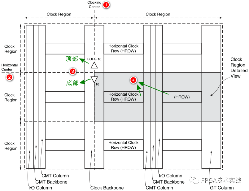
Figure 1, High-Level Clock Structure View of 7 Series FPGAFigure 2 provides a high-level overview of the available clock resources within a clock region and their basic connections.
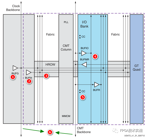
Figure 2, Basic View of Clock RegionIn the figure, we can see:
- The global clock buffer (①) can enter each region through HROW, even if it is not physically located in that region.
- The horizontal clock buffer (②BUFH) drives every clock point in that region through HROW.
- BUFGs and BUFHs share routing paths in HROW (③).
- I/O buffers (BUFIO) and regional clock buffers (BUFR) are located inside the I/O bank (④). BUFIO drives only the I/O clock resources, while BUFR drives both I/O resources and logic resources.
- BUFMR supports multi-region linking of BUFIOs and BUFRs. The clock input (chip *CC pin⑤) connects the external clock to the clock resources on the device. Certain resources can connect to the top and bottom regions via the CMT trunk clock network (⑥).
Figure 3 shows a more detailed view of the clock in a single clock region on the right edge of the device. In this figure, we can see the clock resources that the external clock input pins SRCC and MRCC can drive after entering the I/O Bank, as well as the interconnection of CMT resources with the external clock.
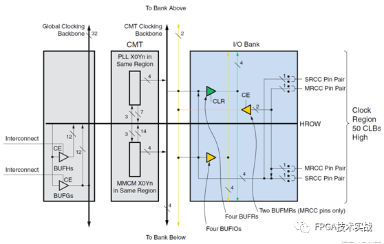
Figure 3, Single Clock Region (Right Side of Device)
Figure 4 shows more detailed connections of global BUFG and regional BUFH/CMT/CC pins as well as the number of available resources within a region (shown here on the right side).
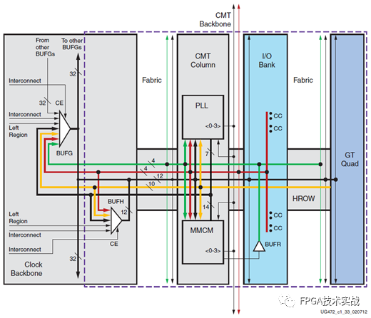
Figure 4, Detailed Connections of BUFG/BUFH/CMT Clock Regions
In Figure 4, we can see:
-
Any one of the SRCC and MRCC clock input pins can drive the PLL/MMCM in CMT and BUFH.
-
BUFG is shown as being located in this region, but can actually be located elsewhere in the clock trunk.
-
BUFG and BUFH share 12 routing paths in HROW, capable of driving all clock points within that region. BUFGs can also drive BUFHs (not shown in Figure 4), allowing independent clock enable (CE) on other global clock distributions.
-
A GT Quad has ten dedicated channels to drive CMT and clock buffers.
-
BUFRs located in the I/O bank have four routing paths driving clock points in logic, CMT, and BUFG. CMT can drive other CMTs in adjacent regions using the CMT trunk network, but this is limited. Similarly, clock input pins can drive CMTs in adjacent regions under the same limitations.
-
Clock input pins can drive BUFG anywhere on the same top/bottom of the device. The CMT trunk network supports four routing paths for vertical region connections.
Logic interconnect drives the CE pins of BUFG and BUFH. Logic interconnect can also drive clocks to the same buffers, but caution must be taken as timing is unpredictable.Figure 5 shows detailed information about BUFR/BUFMR/BUFIO clock regions.
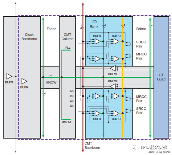
Figure 5, Detailed Information of BUFR/BUFMR/BUFIO Clock RegionsIn Figure 5, we can learn:
- Each I/O bank contains four BUFIOs and four BUFRs. Each of these clock buffers can be driven by dedicated input clock pin pairs (_CC pins) or can be driven directly by specific output clocks from the MMCM.
- Two supporting clock input pin pairs, called MRCCs, support multi-region clock schemes. One MRCC pin pair can drive a specific BUFMR, which in turn can drive BUFIOs and BUFRs in the same and adjacent regions, facilitating multi-region/bank interfaces.
- The GT Quad can also drive BUFMRs.
- MMCM<3:0> outputs have a dedicated high-performance differential path to BUFRs and BUFIO. This feature is also known as High-Performance Clock (HPC).
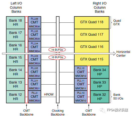
Figure 6, Layout of 7K325T Architecture
Although all 7 series devices have the same basic architecture, there are some architectural differences between series and devices within the series. Each 7 series FPGA has at least one complete I/O column on the left edge of the device. GTs can be any of the serial transceivers supported by the 7 series FPGA (GTP, GTX, or GTH). Devices with GTs either have a mixed column of GTs and I/Os on the right edge of the device (some Kintex-7 devices and some Artix-7 devices), or have a complete GT column on the right edge of the device (some Kintex-7 devices and some Virtex-7 devices) along with a complete I/O column on the right side of the device. Other Virtex-7 devices have complete GT columns on both left and right edges, with complete I/O columns on both sides. Artix-7200t devices have GTP transceivers at the top and bottom of the clock column.
2. Differences between 7 Series FPGA Clocks and 6 Series FPGA
The clocks in the 7 series FPGA have a structure similar to that of the Virtex-6 FPGA and support many of the same functions. However, there are some architectural differences and modifications in the different clock components and their functions. Compared to the Spartan-6 FPGA, there are significant changes in both structure and functionality. Some clock primitives from Spartan-6 FPGA are no longer available, replaced by more powerful and simpler structures.
2.1
Differences from Virtex-6 FPGA
-
The basic BUFIO clock functionality of the 7 series FPGA has not changed, with the only exception being that BUFIO now spans only one Bank. The direct clock of adjacent Banks has been replaced by a new clock buffer. Now each Bank has four BUFIOs, and the basic purpose of BUFR has not changed. However, BUFR now spans only one clock region directly. Now there are four BUFRs and four regional clocks (tracks) in each region.
-
The 7 series FPGA introduces a new buffer type: BUFMR/BUFMRCE. BUFMR/BUFMRCEs drive BUFIOs and/or BUFRs in the same vertically adjacent region. They also provide the same multi-clock region/multi-group clock routing capabilities as the Virtex-6 FPGA’s ability to support the same three clock regions/groups. BUFMRCE has selectable synchronous or asynchronous switching functionality.
-
The 7 series FPGA no longer supports global clock (GC) input pins from the Virtex-6 series. Each column of 4 clock input pins/pairs replaces GCs, and the connectivity of clock input pins has been enhanced to support the previous GC functionality.
-
The global clock multiplexer BUFGMUX adds a property CLK_SEL_TYP, allowing synchronous or asynchronous clock switching between two input clocks (previously only available by ignoring the port).
-
BUFHCE has enhanced clock enable, allowing synchronous or asynchronous enable of input clocks.
-
CMT now contains an MMCM and a PLL (a subset of the MMCM), instead of two MMCMs, along with preserved dedicated memory interface logic. The CMT column is located next to SelectIO™ CMT column/group and has dedicated access to I/O for high performance. Global clock buffers remain located in the vertical center of the device between the I/O columns driven by CMTs. Direct cascading within a CMT is no longer supported. Cascading to adjacent CMTs is possible but limited due to resource constraints. Cascading to other CMTs beyond adjacent CMTs results in phase offsets between source and destination MMCMs/PLLs and requires special attribute settings.
-
Fractional dividers no longer share output counters. This will free these counters for other uses. Fractional counters increase static phase shift capabilities.
-
Clock hold functionality is no longer available
- MMCMs support spread spectrum
2.2
Differences from Spartan-6 FPGA
-
Some clock circuit topologies, functions, and blocks unique to the Spartan-6 architecture are not supported and have been replaced by 7 series FPGA clock functionalities. The 7 series devices do not directly support features and functionalities such as DCM_SP, DCM_CLKGEN, BUFIO2, BUFIO2_2CLK, BUFIO2FB, BUFPLL, and BUFPLL_MCB.
- PLL is a subset of MMCM, with the same performance (except for minimum CLKIN/PFD and minimum/maximum VCO frequency), some connection limitations, and some reduced functionalities. Compared to the previous Spartan® FPGA PLL, the 7 series FPGA PLL adds power-down, input clock switching, and cascading to adjacent CMTs. PLLs do not have direct connections to BUFIO or BUFR.
- In the 7 series FPGA, there is no direct equivalent to BUFIO2 and BUFIO2 clk primitives. It is recommended to use BUFIO and BUFR to replace the connections to drive ILOGIC and Logic.
- The dedicated input routing of Spartan-6 FPGA BUFIO2 from GCLK to CMT and global clock buffers is no longer supported. To migrate to the 7 series FPGA, use dedicated input routing from CCIO pins.
- There is no direct equivalent to Spartan-6 FPGA BUFPLL in the 7 series FPGA. For migration, use BUFIO and BUFR along with recommended connections to ILOGIC and logic. The high-performance clock routing of MMCME2 CLKOUT[0:3] replaces the dedicated routing of BUFPLL.
- BUFIO2FB primitives are no longer needed in the 7 series FPGA. For feedback connections of MMCM and PLL, CLKFBIN can be directly connected to global clock buffers, input pins, or CLKFBOUT, depending on the feedback used.
- Only BUFH is supported in the Spartan-6 FPGA. The 7 series FPGA BUFHCE primitive adds the ability to disable the clock for potential power savings in the clock region driven by that resource.
- The new buffer BUFMR/BUFMRCE in the 7 series FPGA drives BUFIO and/or BUFRs in the same and vertically adjacent clock regions. When used with BUFIO or BUFR, BUFMR/BUFMRCE allows MRCC input access to BUFIO and BUFR regions in adjacent clocks. BUFMRCE has selectable synchronous or asynchronous switching functionality.
- A new primitive for migrating Spartan-6 FPGA designs is BUFR. When used with BUFIO, BUFR functionality replaces BUFIO2, BUFIO2 clk, and BUFPLL functionalities. There are four BUFRs in each clock region.
- Another new primitive for migrating Spartan-6 FPGA designs is BUFIO. When used with BUFR, BUFIO functionality replaces BUFIO2, BUFIO2 clk, and BUFPLL functionalities.
- Unlike the two DCMs and one PLL in the Spartan-6 architecture, the CMT used in the 7 series FPGA contains an MMCM, a PLL, and dedicated memory interface logic, which is reserved for Xilinx at this time. These functions now support DCM and its associated functionalities. The CMT is located in a separate column adjacent to the SelectIO column, with dedicated access to I/O. DCM_SP and DCM_CLKGEN are no longer available, and their functionalities are now supported in MMCMs and PLLs.
- The 7 series FPGA no longer supports global clock (GCLK) inputs. Now, each bank supporting the GCLK pin functionality of Spartan-6 FPGA has four supporting clock input pins.
- For Spartan-6 FPGA designers, MMCM is a new functional block. MMCM adds features such as frequency division, fine phase shifting, dynamic phase shifting, inverted clock output, cascading CLKOUT6 to CLKOUT4, and several other functions. Using CLKOUT[0:3], HPC connections from MMCMs to BUFIO/BUFR replace the direct routing connections to BUFPLL. A broader DRP is also provided.
- Using PLL is no longer the recommended CMT functionality for general high-speed I/O clocks. PLLs do not have direct connections to BUFIO or BUFR. CLKOUT0 feedback is no longer supported. Use MMCM for high-speed I/O interfaces. Cascading connections use limited CMT trunk resources. There is also a new power-down mode. Input clock switching is fully supported. The operating ranges of Spartan-6 FPGA and 7 series FPGA differ. DRP functionality is still available. The positions and addresses of DRP functionality have changed.
- Spartan-6 FPGA DCM_SP is no longer supported. For migration to 7 series FPGA, use MMCM and PLL.
- Spartan-6 FPGA DCM_CLKGEN is not directly supported in the 7 series FPGA. Use MMCM or PLL for low-bandwidth input jitter filtering. The DRP reference design of MMCM or PLL can also be used to dynamically reprogram M/D values.
3. Overview of Clock Connections
Table 1 summarizes the clock connections in the 7 series FPGA.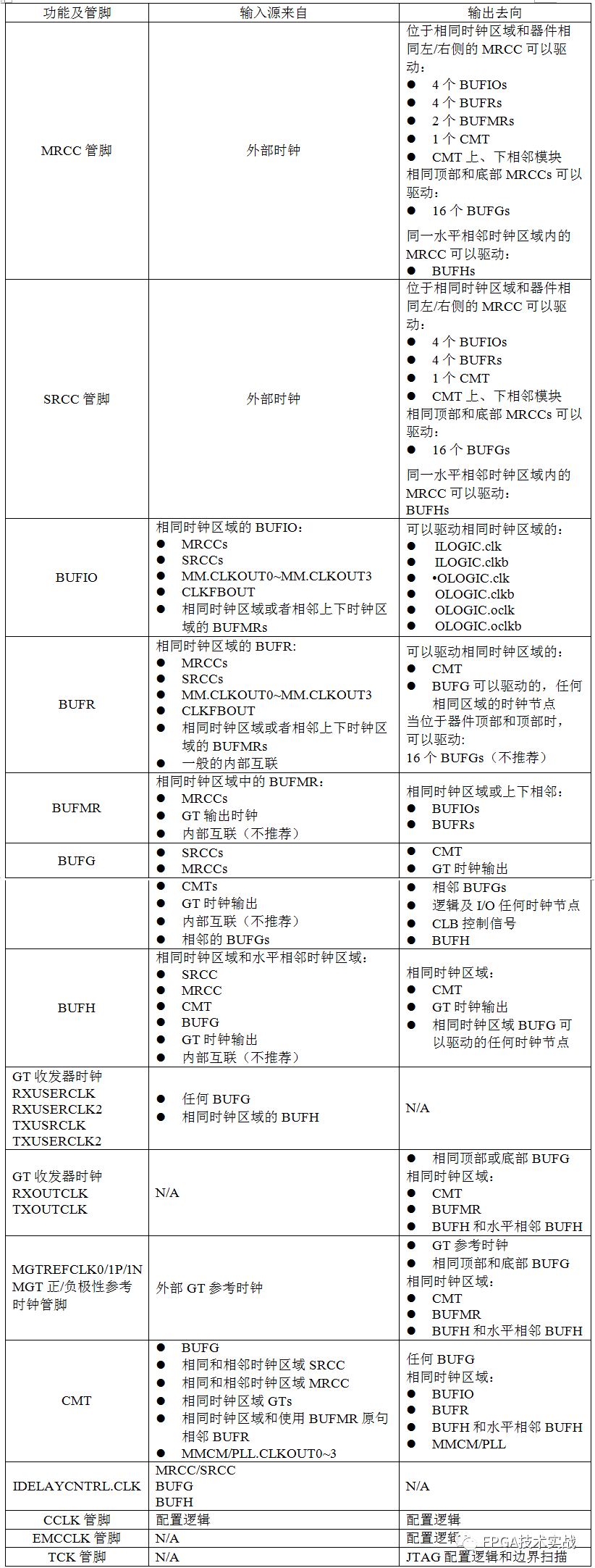 Table 1, Summary of Clock Connections in 7 Series FPGA
Statement:
This account maintains neutrality in the statements and views of all original and reprinted articles, and the articles pushed are for readers’ learning and communication purposes only. The copyrights of articles, images, etc., are owned by the original authors.
For submissions/recruitment/promotion/publicity, please add WeChat: 15989459034