
Recently, the first domestic wafer service platform for fully localized silicon photonic PDK (Process Design Kit), TDK (Test Design Kit), and ADK (Assembly Design Kit) based on a 12-inch 40nm CMOS process line was officially put into operation in the Optics Valley. This platform is constructed and operated by the National Information Optoelectronics Innovation Center (NOEIC), marking another key breakthrough for the center in the field of silicon photonics.
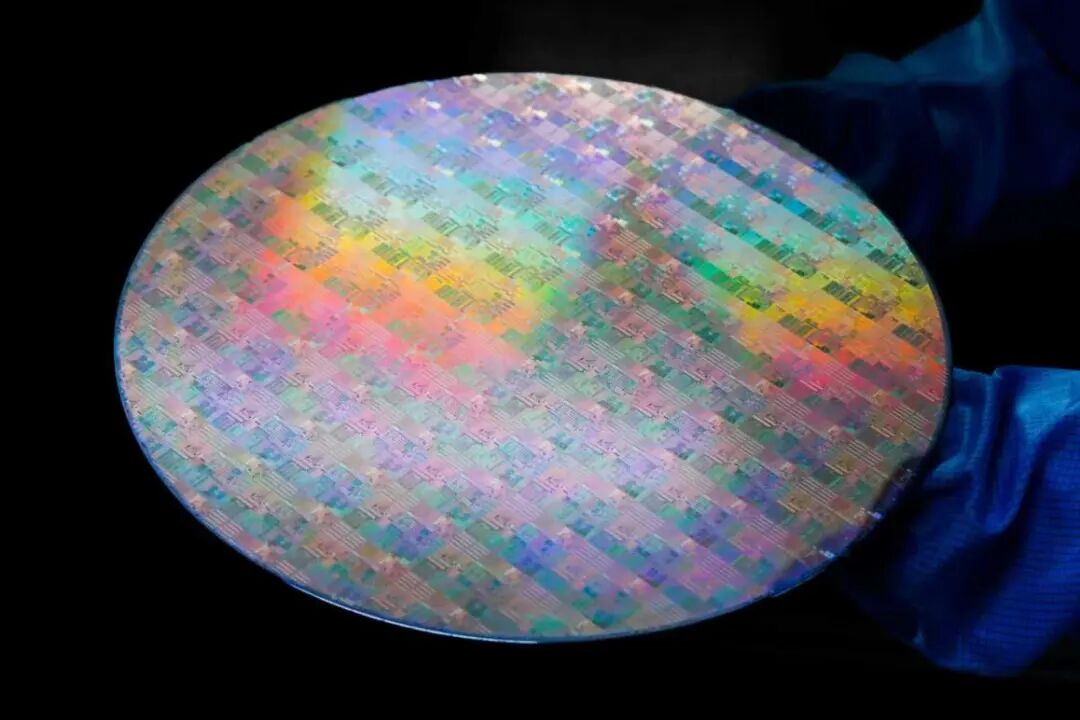 Silicon photonic chips from the National Information Optoelectronics Innovation Center
Traditional chips rely on electronic data transmission, akin to trucks transporting goods. In contrast, silicon photonic chips allow photons to traverse through optical fibers, transforming into a “light-speed high-speed train.” In recent years, with technological maturity and the explosive demand from AI, silicon photonic chips have seen large-scale applications in cutting-edge industries such as artificial intelligence and big data. Leading consulting firm LightCounting predicts that by 2030, silicon photonic chips will account for 60% of the optical communication chip market.
The National Information Optoelectronics Innovation Center was established in 2018 in Optics Valley, tasked with solving key common technology challenges in China’s information optoelectronics manufacturing industry and facilitating the first commercial applications.Over the past seven years, it has supported over 300 units, completed more than 800 orders, and achieved breakthroughs in key technologies such as 1.6T silicon photonic interconnect chips, 2T chiplets, and 145GHz intensity modulators.
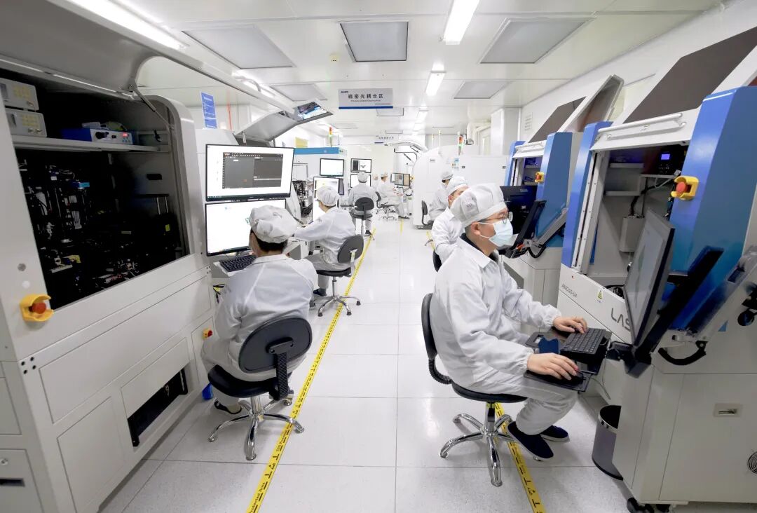
Work scene at the National Information Optoelectronics Innovation Center
East Lake High-tech Zone is proactively supporting the construction of a 12-inch silicon photonic chip development service platform at the National Information Optoelectronics Innovation Center by providing stable, open, and comprehensive MPW (Multi-Project Wafer) wafer service, promoting the industry from “single-point breakthroughs” to “clustered and scaled development.”
This platform innovatively constructs a silicon photonic MPW service model by integrating multiple chip designs onto the same wafer, achieving cost-sharing and significantly lowering the R&D threshold. The platform’s silicon photonic PDK1.0 based on a 40nm process meets commercial requirements, with its processing accuracy, waveguide loss, and optical coupling efficiency reaching internationally advanced levels. In addition to the PDK, the platform also integrates TDK and ADK, providing full-process support from integrated design to packaging verification, meeting the rapid iteration needs in research result transformation and product development, and facilitating project acceleration.
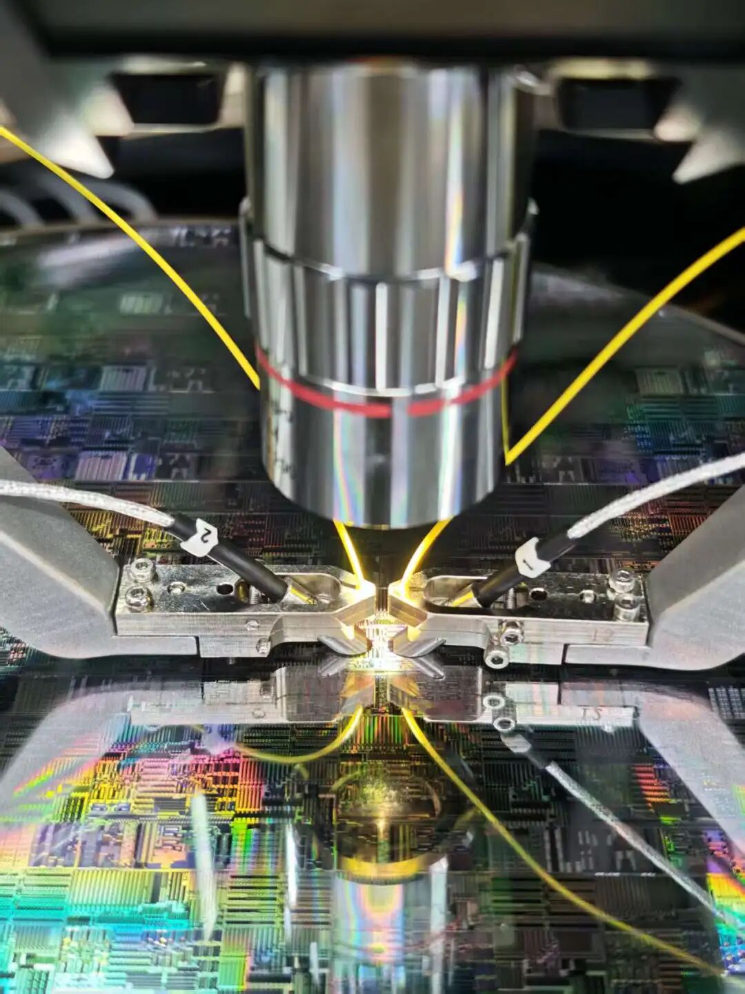
Silicon photonic chip processing scene at the National Information Optoelectronics Innovation Center
Currently, Optics Valley is targeting two major goals: “World Capital of Storage” and “Global Compound Semiconductor Industry Innovation Center,” having established a “3+2” integrated circuit industry system dominated by storage integrated circuits, compound integrated circuits, and 3D integration, with advanced packaging and silicon photonic integrated circuits as features. Plans are underway to build a 7 square kilometer storage industry innovation district and a 14 square kilometer compound semiconductor industry innovation district, providing 1 million square meters of high-standard factory space annually, with the integrated circuit industry scale expected to exceed 80 billion yuan by 2024, continuously enhancing industry influence and global impact.


Welcome to follow the APC Global Fiber Optic Cable Conference.
WeChat Subscription Account: APC-GOFC
Chinese Website: http://www.apofc.cn

Welcome to follow the “Global | China Optical Communication Most Competitive Enterprise Selection Activity.”
WeChat Subscription Account: NetworkTelecom
Website: www.networktelecom.cn