According to news from China Optics Valley, the first domestic fully integrated silicon photonics PDK (Process Design Kit), TDK (Test Design Kit), and ADK (Assembly Design Kit) wafer service platform based on a 12-inch 40nm CMOS process line has officially been launched in Optics Valley. This platform is operated by the National Optical-Electronic Innovation Center (NOEIC) and marks another key breakthrough for enterprises in the silicon photonics field.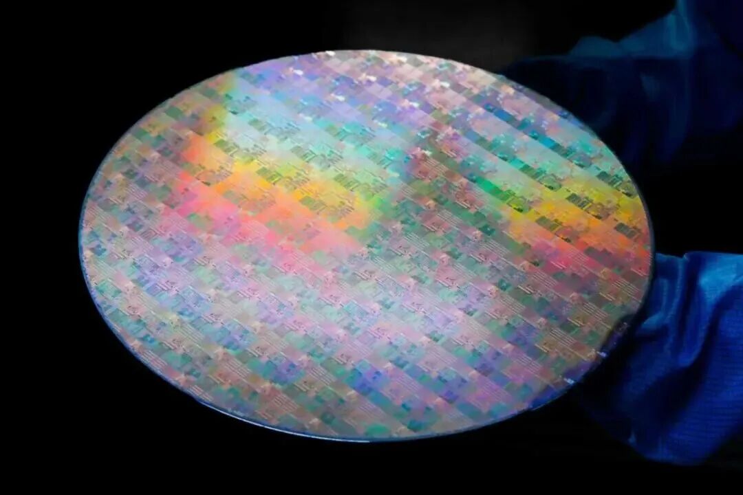
(Silicon photonics chips from the National Optical-Electronic Innovation Center, source: China Optics Valley)
The National Optical-Electronic Innovation Center was inaugurated in Optics Valley in 2018, tasked with solving key common technology challenges in China’s optical-electronic manufacturing industry and facilitating the first commercial applications. Over the past seven years, it has supported over 300 units, completed more than 800 orders, and achieved breakthroughs in key technologies such as 1.6T silicon photonic interconnect chips, 2T chiplets, and 145GHz intensity modulators.
The Donghu High-tech Zone has proactively supported the construction of the 12-inch silicon photonics chip development service platform by the National Optical-Electronic Innovation Center. By providing stable, open, and comprehensive MPW (Multi-Project Wafer) wafer service, it promotes the industry’s transition from “single-point breakthroughs” to “clustered and scaled development.” This platform innovatively constructs a silicon photonics MPW service model, integrating multiple chip designs onto the same wafer, achieving cost-sharing and significantly lowering the R&D threshold.
The platform’s silicon photonics PDK 1.0, based on a 40nm process, meets commercial requirements overall, with processing accuracy, waveguide loss, and optical coupling efficiency reaching internationally advanced levels. In addition to the PDK, the platform also integrates TDK and ADK, providing full-process support from integrated design to packaging verification, meeting the rapid iteration needs in research results transformation and product development, thus accelerating project implementation.
It is reported that the challenges faced by domestic silicon photonics chip wafer services are a systemic problem that is interlinked. In today’s increasingly mature sharing economy, MPW services are becoming one of the most realistic and critical strategies to solve the current domestic silicon photonics wafer service dilemma. MPW achieves cost-sharing by integrating multiple process-compatible chip designs onto the same wafer, significantly lowering the R&D threshold for small and medium-sized enterprises and research institutions.
For universities and startups, MPW distributes the originally high costs of mask and wafer manufacturing across dozens of design projects, reducing the cost of a single wafer run to one-tenth or even lower, strongly supporting the ongoing development of research and small-scale innovation. For design companies, MPW allows them to conduct multiple design iterations at lower costs, quickly validate design concepts and IP modules, and accelerate technology maturity, thus encouraging more investment in frontier exploration. Meanwhile, foundries accumulate valuable process data while handling diverse designs, continuously feeding back to improve the PDK and stabilize the process, forming a virtuous cycle of “the more wafers produced, the more mature the process.”
–——-
Source: Official Media/Online News. Please delete if infringing.