As an embedded engineer, everyone should know about download debuggers. But do you really understand the meaning and differences of the SWD and JTAG interfaces?
What is a Download Debugger?
In simple terms, a download debugger is a device that converts commands sent from a PC (e.g., via USB protocol) into a language understood by the MCU (which controls the internal peripherals of the MCU) (e.g., SWD or JTAG protocol), allowing for code loading and precise execution control.
Debugger Protocol Standards
In simple terms, a standard is a set of rules and protocols that every participant in a specific industry agrees to follow and implement.
2. The Chaos of Debugger Protocols
Before protocols like SWD and JTAG emerged, the debugger and its protocols were chaotic, with each MCU manufacturer proposing its proprietary methods for loading code onto their MCUs. Every time a manufacturer released a new MCU, embedded software engineers needed to understand its proprietary protocol to load code onto the microcontroller.
Moreover, debugging adapters are expensive because manufacturers effectively have no competitors to match debugging adapters with their proprietary protocols. Another reason for their high cost is due to their limited availability, as they can only sell debugging adapters to companies (engineers) using their manufactured MCUs.
Different protocols also lead to increased development costs. For example, if you have four different chips from four different manufacturers on the board you are designing and wish to conduct some automated testing to improve production efficiency, you need to create a super complex production code that can adapt to the complexity, and install four different debuggers at test points on the circuit board, increasing costs, production time, and programming time.
3. Establishing Protocols
Various download debugging differences can lead to several issues:
• More time spent on learning
• Increased costs for downloading and debugging
• Inefficient test generation
To address this issue, engineers from major MCU manufacturers have established some standard protocols for debugging.
JTAG:Joint Test Action Group, formed to address testing issues.
This group began discussions in the late 1980s and officially released documentation interpreting the IEEE standard in 1990. (IEEE stands for the Institute of Electrical and Electronics Engineers, an international organization that publishes all standards, such as WiFi, Bluetooth, etc.). The protocol they proposed was recorded in IEEE 1149.1 in 1990. The document has since been revised and improved, and as of this writing, the latest standard is IEEE 1149.7.
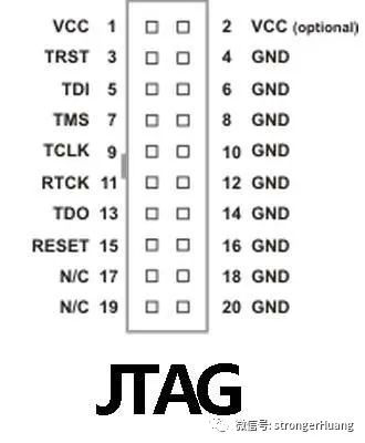
JTAG basically has 5 pins:
• TDI (Test Data In): Serial input pin
• TDO (Test Data Out): Serial output pin
• TCK (Test Clock): Clock pin
• TMS (Test Mode Select): Mode select (control signal) pin
• TRST (Test Reset): Reset pin
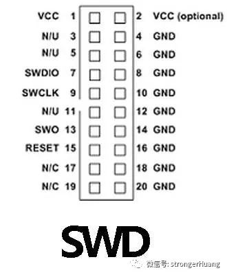
SWD:Serial Wire Debug, a protocol designed by ARM for programming and debugging its microcontrollers.
Since SWD is specifically designed for programming and debugging, it has many special features that are often unavailable elsewhere, such as sending debugging information to a computer via the I/O lines. Additionally, because it is specifically manufactured by ARM for use in its devices, the performance of SWD is often the best among its peers!
• SWDIO (Serial Wire Data Input Output): Serial data input/output pin
• SWCLK (Serial Wire Clock): Serial wire clock pin
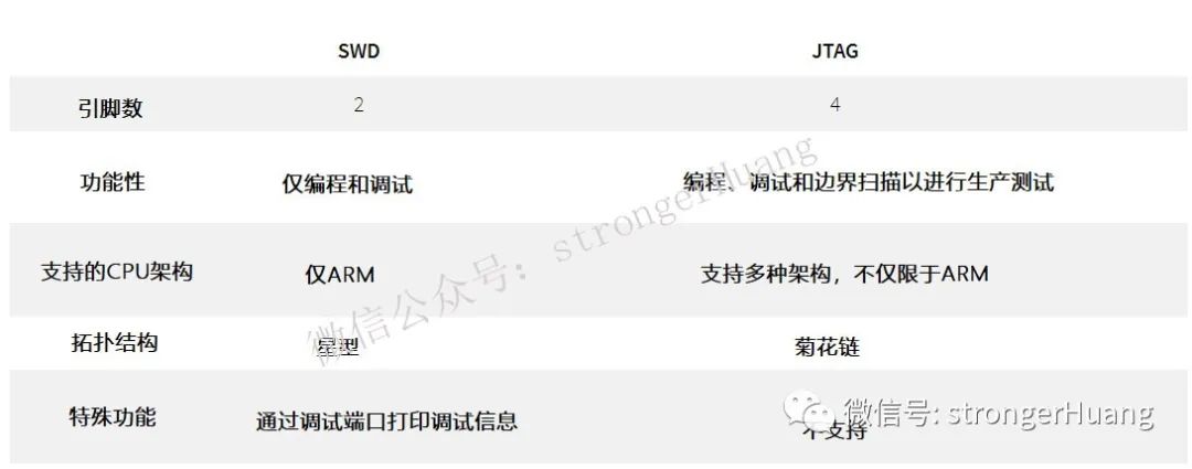
Differences Between SWD and JTAG
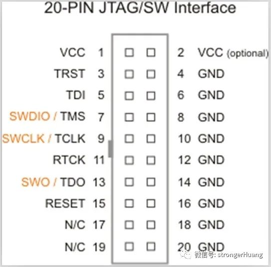
There are many MCUs and debugging adapters on the market that are compatible with both SWD and JTAG protocols. They typically achieve download and debugging functionality through a set of download debugging pins, which are internally multiplexed to SWD and JTAG peripherals.
The pins of SWD can be reused with JTAG pins under certain conditions. Currently, there are many connectors for SWD and JTAG, such as the 20-pin connector:
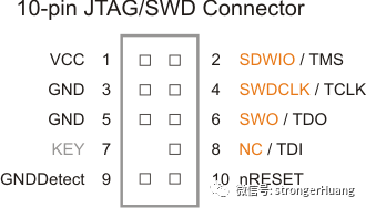
Of course, there are also 10-pin connectors:
2. Advantages of SWD and JTAG
Advantages of SWD Protocol:
• Uses fewer pins, requiring only SWDIO and SWCLK;
• SWD has special features, such as printing debugging information through its I/O lines;
• SWD generally has better overall performance in speed compared to JTAG.
Advantages of JTAG Protocol:
• JTAG is not limited to ARM chips; it also supports chips outside of ARM, such as the familiar MSP430;
• JTAG has more varied uses for programming, debugging, and production testing;
• JTAG is an independent group that evolves with the development of the protocol.
When to Choose SWD Over JTAG:
• If your schematic/circuit board design is simple enough to test without JTAG functionality;
• Debugging performance is more important than production testing, and your device focuses on research rather than mass production;
• The MCU has size constraints, and SWD can save space;
• Your hardware design is too complex, and the MCU has no extra two pins.
Below is a diagram to summarize:
Copyright belongs to the original author. If there is any infringement, please contact for deletion.
Step-by-step Guide to Setting Up STM32 Development Environment in VSCode
God’s Explanation: The Four Major Communication Interfaces: UART, I2C, SPI, 1-wire
Why Are Chinese Numbers Four Digits and Western Numbers Three Digits?
→ Follow for More Updates ←