0 Introduction
CPU design is an important experimental content in the course of computer organization principles, and it is a crucial part of cultivating the capabilities of computer systems. Many universities both domestically and internationally have included CPU design in their computer organization courses [1-2]. Since CPU design involves numerous core components such as the arithmetic logic unit, control unit, registers, memory, as well as system mechanisms like data paths and interrupts, along with the writing of high-level language code in C, it requires a comprehensive understanding of many knowledge points. The connections between these points are intricate and complex, making it somewhat challenging for entry-level students in general universities, which can be daunting for them. The CPU simulation design method based on Dream Logic combines the experimental content of computer organization principles with simulation applications and practices using assembly instructions such as MOV, ADD, and JMP. The CPU design is conducted in a component-module-system manner, involving the drawing of hardware schematics and the writing of software code, integrating digital circuits and computer organization principles into a single entity, serving as a helpful tool for students learning CPU design and conducting hardware simulation experiments.
1 Dream Logic Simulation Tool
Dream Logic is a high-performance virtual software fully integrated into CodeCode.net (a new engineering construction platform for computer majors), featuring powerful simulation development and design capabilities, mainly reflected in: ① It provides a rich library of digital and analog devices, digital chips, and logic gates, meeting the design needs of circuits and systems of various scales. Users can easily and quickly draw their own components or schematics according to their needs; ② It offers component modules such as registers, bus transceivers, memory, and buses, as well as sub-functional modules like processors and pipelines designed with these components. Each module can be used independently and reused multiple times. Users can simulate applications with these modules or design all components and modules according to their needs; ③ It has fully visual interactive simulation capabilities. Through interactive controllers, users can modify and select high and low-level digital sources in the circuit and single-step clock at any time. They can monitor the working status and various operational states of the circuit using visual means such as digital probes, digital tubes, and logic analyzers, allowing for quick identification of error causes; ④ It provides open-source instruction assemblers and micro-instruction assemblers written in C for the 8086 and MIPS processors. Users can add their designed assembly instructions and micro-instructions by modifying the source code, and they can also write new assemblers and micro-instructions; ⑤ It can be used for simulation experiments in courses like “Digital Logic” and “Computer Organization Principles,” and can also be used for course design, graduation projects, and other innovative designs and developments by developing components or integrating modules.
2 CPU Simulation Design
2.1 Overall Design
The overall structure of the CPU design is shown in Figure 1, where the hardware part adopts a bottom-up modular design method, including seven major modules: arithmetic logic unit, control unit, register group, program counter, memory, hardware interrupt controller, and input/output. Each module is mainly composed of logic gates and functional chips, and the modules are connected according to the principles of synchronous sequential circuits through an 8-bit data bus and address bus. The register group module is used to store operands temporarily used during instruction execution or intermediate results and final results generated during operations. The arithmetic logic unit module is responsible for performing core arithmetic operations such as addition, subtraction, and shifting. The control unit module coordinates and directs the operations of the entire model machine through multiple control signals. The program counter module ensures the sequential execution or jump execution of the program. The memory module consists of one RAM chip and one bus transceiver, used to store instructions, data, and test case programs used during program execution. The hardware interrupt controller module simulates the process of interrupt handling, consisting of an interrupt request register, priority discriminator, and interrupt service register. The input/output module simulates the connected external devices, achieving input/output functionality [3-4].
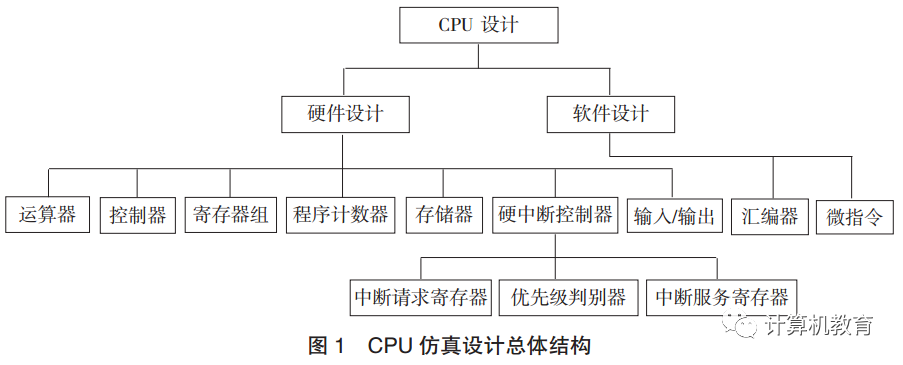
The software part mainly includes the design of the assembly instruction system, assembler, and micro-instruction functional modules.
2.2 Arithmetic Logic Unit Design
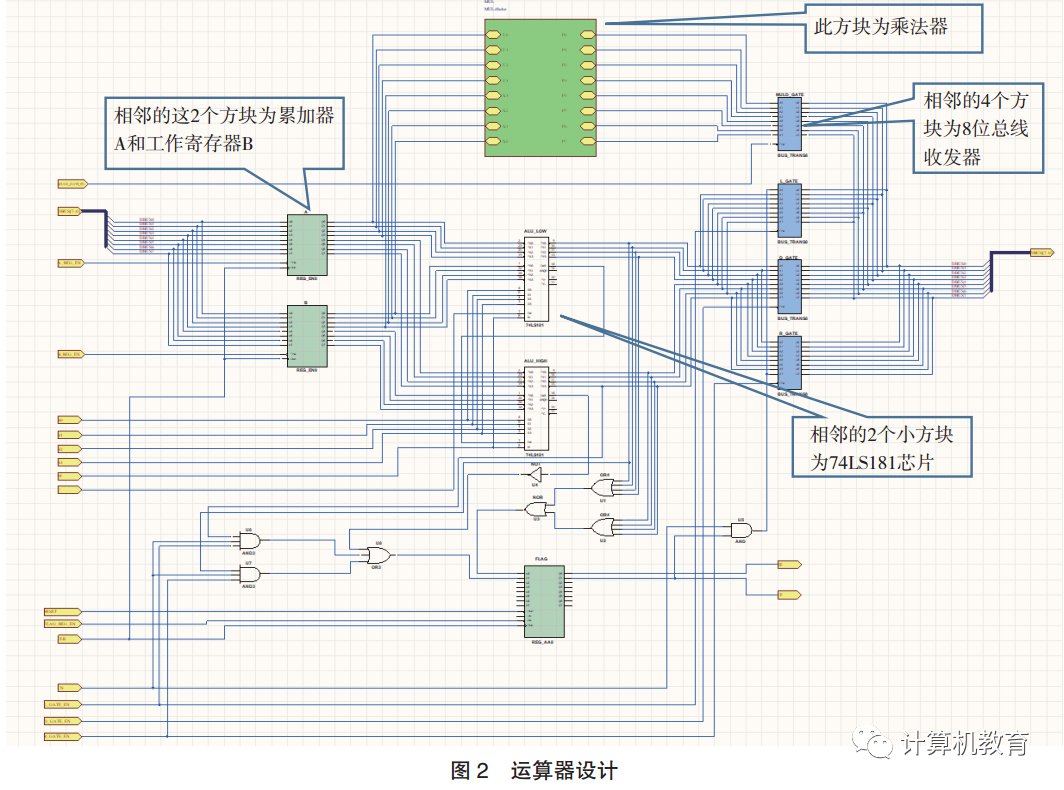
The main function of the ALU module is to perform arithmetic, logical operations, and shifting operations for instructions. It mainly consists of two data registers A and B, two 4-bit 74LS181 chips, a dedicated multiplier, a flag register, and some logic gates (as shown in Figure 2). Registers A and B store the operands needed for operations, with their input terminals connected to the data bus, the enable terminals connected to A_REG_EN and B_REG_EN signals respectively, and the low 4 bits of the output connected to the input terminals of the first 74LS181 chip, while the high 4 bits are connected to the input terminals of the second 74LS181 chip. The two 74LS181 chips can perform 8-bit operations through cascading, and their output terminals are connected to the data bus via the bus transceiver D_GATE. The flag register contains two flags: CF (carry flag) and ZF (zero flag), with its clear terminal connected to the RESET signal, the enable terminal connected to the Flag_REG_EN signal, and the low 2 bits of the input connected to the final calculated ZF and CF values, while the low 2 bits of the output are connected to ZF and CF signals.
2.3 Instruction System Design
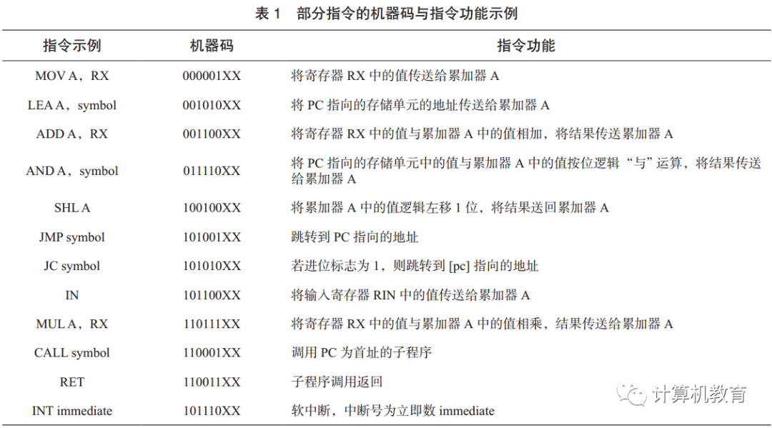
The instruction system is the starting point and basic basis for CPU design, closely related to the complexity of the hardware structure [5]. The core issue in designing the instruction system is the selection of instruction formats and functions, involving addressing modes and instruction encoding formats [6]. The addressing modes in this design include immediate addressing, register addressing, direct addressing, and register indirect addressing; the designed instructions include 54 instructions such as arithmetic operation instructions, data transfer instructions, bit manipulation instructions, and transfer instructions. The design idea of this instruction system is that the machine code for most instructions is single-byte, while some are double-byte. Regardless of whether it is single-byte or double-byte, the high 6 bits of the first machine code byte are fixed as the opcode, and the low 2 bits are the address code, used to represent the selected register number. The 6-bit opcode can encode 64 instructions, but only 59 instruction encodings are used this time. Additionally, because the micro-instructions for INT (software interrupt), hardware interrupt, LEA, and CALL are too long, occupying 2 instruction encodings, a total of 54 instructions have been designed. Table 1 shows a selection of machine codes and their corresponding instruction functions as examples, with the remaining 5 opcodes reserved for future innovative designs to add new functionalities.
The micro-instructions used in this design include data transfer micro-instruction path, placeholder micro-instruction dup, null micro-instruction null, target operand increment micro-instruction inc, reset micro-instruction reset, and after each instruction execution, there are micro-instructions to check for interrupt requests ask_for_int, record interrupt numbers inta1, read interrupt numbers into the interrupt vector register IA inta2, and clear the flag bits in the interrupt service register ISR eoi. Among these, path and dup micro-instructions contain 2 operands, while inc and reset micro-instructions contain 1 operand, and null, ask_for_int, inta1, inta2, and eoi micro-instructions have no operands. Through these micro-instructions, the combinational devices can achieve the functionality of all assembly instructions. When writing the micro-instruction program, it is important to ensure that the first operation executed by all instructions is the fetch operation, which can be understood as the 0th instruction being the fetch instruction. Additionally, it must be ensured that the entry address of each instruction’s corresponding micro-instruction is a multiple of 8. If there is an instruction whose corresponding micro-instruction count is less than a multiple of 8, it needs to be supplemented with the placeholder micro-instruction dup.
2.4 Micro-Instruction Design
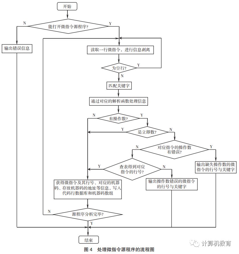
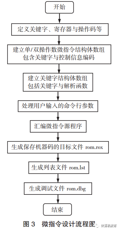
The function of the micro-instruction is to process the micro-instruction code, generating control signal encoding files stored in read-only memory (ROM) and debugging files displayed during simulation [7-8]. Each micro-instruction occupies 4 bytes, with different control signals corresponding to each. The entry address of each instruction’s micro-instruction must correspond to the high 6 bits of the instruction machine code. The micro-instruction codes in this design are written in C language (2017 version), and the design flowchart is shown in Figure 3. The generated target file rom.rxm stores control signal encodings, the list file rom.lst contains each micro-instruction along with its line number, control signal encoding represented by the micro-instruction, and the address where the micro-instruction is stored; the debugging file rom.dbg contains the model number, version number, source code, and the path of the list file, as well as all content in the code line database. The processing flow is shown in Figure 4.
3 CPU Application Practice
3.1 Arithmetic Logic Unit Experiment
The arithmetic logic unit module mainly consists of two 4-bit arithmetic logic units 74LS181 [9-10], and the functions of the 74LS181 are shown in Table 2.
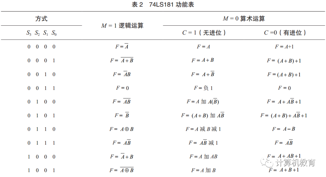
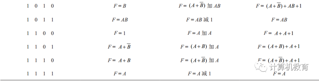
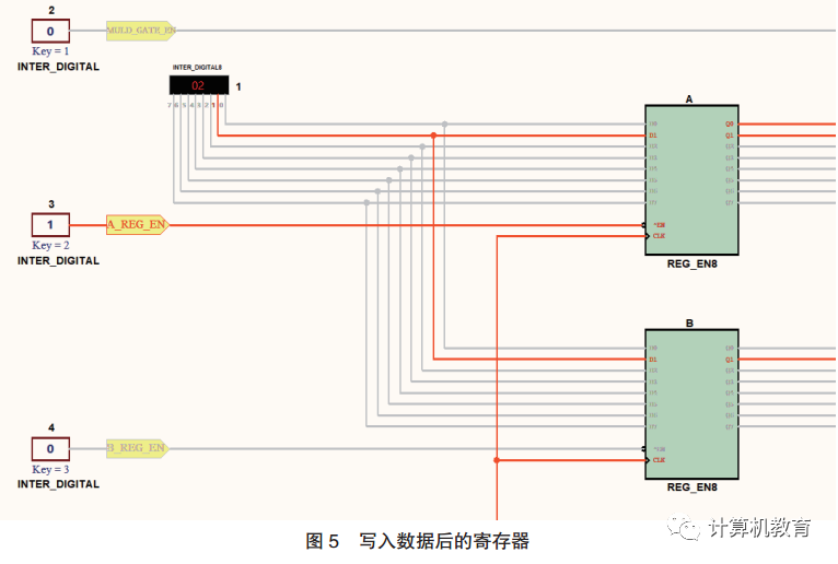
This experiment takes the example of calculating the sum of 3 + 2 as a carry-free addition arithmetic operation. In the 8-bit data input source, input 3, set A_REG_EN to 0, B_REG_EN to 1, and provide one clock rising edge to write data 3 into accumulator A; then set A_REG_EN to 1, B_REG_EN to 0, and write data 2 into working register B. The schematic of the registers after writing data is shown in Figure 5.
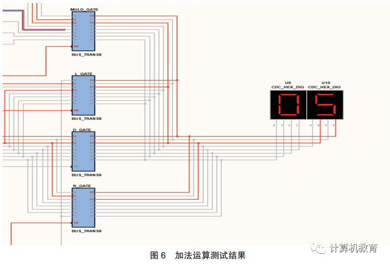
To perform carry-free addition, according to the rules in Table 2, first set the S3~S0 signals to 1001, set the M signal to low level 0, and set the C signal to high level 1. Then change the signal input source, set the data output tri-state gate enable signal to 0, making the enable signals of accumulator A and the flag register effective, while setting the other tri-state gate signals to 1 [11]. At this point, the operation result can be seen at the data output terminal, as shown in Figure 6.
3.2 CPU Model Machine Experiment
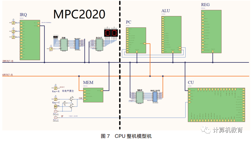
The completed CPU model machine after simulation design is shown in Figure 7, and computer organization principles application practice is conducted based on this model machine, with the example program source code shown in Figure 8.
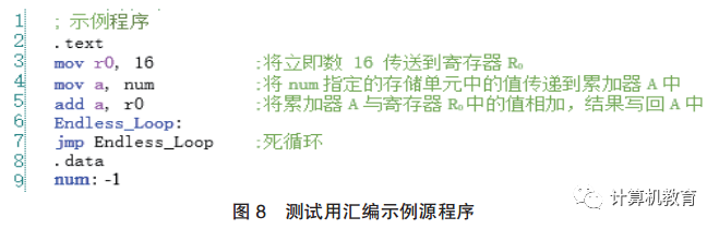
The function of this example program is to add the immediate value 16 to the data -1 stored in a specified storage unit, and store the result 15 (0FH) in accumulator A. The opcodes involve MOV transfer instructions, ADD arithmetic operation instructions, and JMP transfer instructions, while the operands involve register R0, immediate value 16, accumulator A, and the storage unit defined by num. Before running, the source program must be assembled by the assembler, and the generated target code is written into the main memory (as shown in Figure 9). In the simulation working interface of Dream Logic, there are two code windows: one is the “Source Code 1” window (for storing the test program in random access memory RAM1), and the other is the “Source Code 2” window (for storing the micro-instructions in read-only memory ROM), with two arrow cursors pointing to the currently executing instruction code and micro-instruction code respectively.
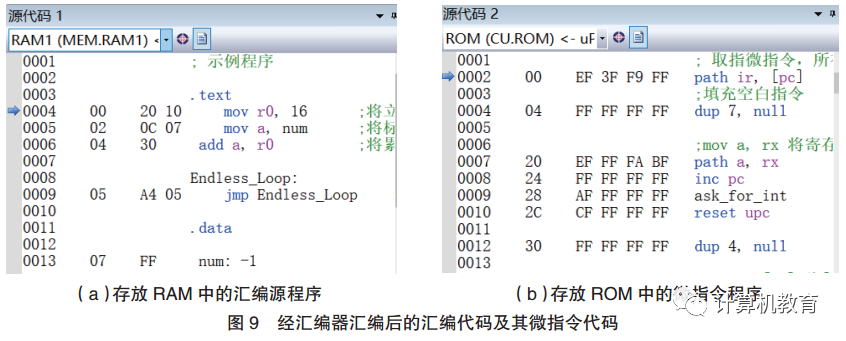
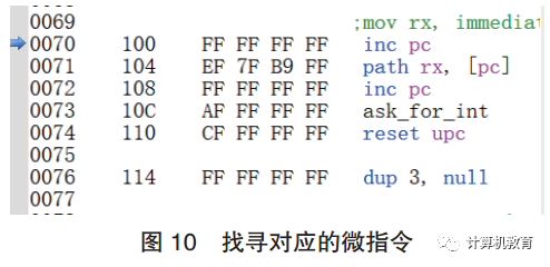
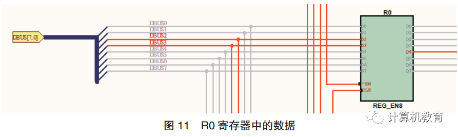
Operation process: In the initial state without providing a high level, the cursors at the assembly source code and micro-instruction source code both stay at the first instruction (as shown in Figures 9(a) and 9(b)); set key 1 to high level (indicating single-step operation), set key 2 to low level (disallowing interrupts), with the current PC at 00H, corresponding to the fetch micro-instruction operation. If a clock rising edge is provided (key C), it points to instruction encoding 20H, the controller obtains the instruction encoding, finds the corresponding micro-instruction entry address 100H for mov rx, immediate (as shown in Figure 10), and completes the corresponding micro-instruction operation. When key C is pressed again to provide a clock rising edge, uPC+1 (executing inc pc micro-instruction) points to the next micro-instruction, at this point PC is 01H, corresponding to the operand encoding of immediate value 16 (10H). Pressing key C again executes the “path rx, [pc]” micro-instruction, transferring the data stored in 01H (10H) to register R0, and continue pressing key C until the “reset uPC” micro-instruction is executed, resetting uPC and returning to the fetch operation, at which point PC becomes 02H, corresponding to the instruction encoding 0CH. Thus, the first instruction of sending data 16 into register R0 is completed, and the execution result is shown in Figure 11.
Following this principle, sequentially execute the second, third, and the last instruction jmp Endless_Loop.
4 Practical Experience and Outcomes
Our university introduced the Dream Logic simulation tool in 2016 and combined it with physical experimental boxes for the experimental courses in computer organization principles. As a comprehensive experiment in the course, CPU design plays a crucial role in both theory and practice. The teaching experiences are as follows.
(1) The graphical interface provided by Dream Logic is quick and convenient, allowing users to call upon over 100 commonly used analog and digital devices at will. The operation and debugging are simple and convenient, with experimental results being clear and easy to understand. Students gain a sense of achievement through successful experiments, which greatly enhances their interest in experiments.
(2) The simulation effects of virtual devices in Dream Logic are realistic and accurate. For example, light-emitting diodes can emit red, yellow, and green light, logic probes can directly display the high and low levels of circuit nodes like logic pens, relays and switches can operate their contacts, fuses can blow, bulbs can burn out, buzzers can produce different tones, and potentiometer contacts can proportionally move to change resistance values. Students can better understand the execution process of hardware operations and the data flow between modules, leading to high experimental transparency and a tangible feel of real components.
(3) Using Dream Logic helps cultivate systematic capabilities. For example, the design of the instruction system is not just about implementing the functionality of a single instruction, but also relates to the designer’s understanding of the overall structure, the invocation and implementation of each component’s functionality, the execution flow of instructions, and the design of various control signals, as well as the programming application of C code. This truly integrates software and hardware design, achieving a comprehensive learning experience in digital logic and computer organization principles. [12]
(4) The “virtual simulation + physical implementation” experimental model overcomes the inherent limitations of traditional physical experimental boxes, such as fixed circuit structures and spatial-temporal constraints, limited resources, high costs, high losses, and low lifespans, making it difficult for students to engage in detailed design and expansion. It effectively leverages the capabilities of simulation tools to expand experimental space, extend experimental time, and provide more flexible and convenient conditions and means for students to conduct innovative or research-oriented experiments [13].
So far, our university has applied Dream Logic in the computer organization principles course for five cohorts of computer and information security majors, achieving satisfactory teaching results. This is mainly reflected in: ① The passing rate of the computer organization principles course has increased from less than 5% under the traditional experimental model to 11%, while the failure rate has decreased from nearly 20% to 4%. ② For the comprehensive experiment of CPU design, students have invested great enthusiasm and energy from searching for information to designing and validating schemes, to final debugging. Groups often argue passionately over a single issue, and they frequently remain reluctant to leave the laboratory even at meal times. The number of instructions designed by students has also increased year by year. ③ In terms of participation in innovation and entrepreneurship projects, competitions, and graduation projects, the number of students choosing computer hardware topics has increased from being rare to now accounting for 35% of the total topics. Over the past five years, computer science students have consistently been on the list of first prizes in the “Electronic Design Competition” organized by the school; students have also won various first and second prizes in competitions organized by Tianjin Qicheng Technology and other units. ④ From the experimental reports written by students, it can be seen that after completing the comprehensive CPU design experiment, students generally feel a sense of pride and achievement, no longer fearing hardware design and low-level software development.
5 Conclusion
This CPU simulation design still has some shortcomings, such as the virtual device inventory only includes a logic analyzer, and the CPU simulation only implements the design of an 8-bit model machine. Based on this, we will continue to research and develop more practical devices, such as digital ammeters, digital voltmeters, digital multimeters, digital storage oscilloscopes, digital function generators, digital signal generators, and devices that can directly display circuit frequency response such as Bode plotters and digital signals. We will also continue to research and practice the design of 16/32-bit CPUs and even multi-cycle multi-stage pipeline MIPS processors. On the basis of writing assemblers and micro-instruction codes, we will encourage students to design compilers themselves, integrating the simulation platform into hardware courses such as “Microcomputer Principles and Interface Technology” and “Computer Architecture,” laying a solid foundation for effectively integrating multiple core courses in computer science—digital logic + computer organization principles + assembly language + operating systems + compiler principles.
References:
[1] Wang Lisheng, Yu Zhiming, Zhang Dongdong. Research on CPU Design Methods in the “Computer Organization Principles” Experiment [J]. Experimental Technology and Management, 2018, 35(5): 1-5, 9.
[2] Wu Jiming, Zeng Biqing. An Efficient CPU Design Method and Its Application in the Course of Computer Organization Principles [J]. Laboratory Research and Exploration, 2018, 37(9): 147-153.
[3] Xu Aiping, Zhang Yuping, Tu Guoqing. CPU Design and Practice Based on VHDL [J]. Laboratory Research and Exploration, 2014, 33(5): 120-124.
[4] Wang Yujian, Zhu Baosong, Liu Yuyan, et al. Exploration of the Design and Implementation of a 16-bit CPU Based on VHDL [J]. Journal of Kunming University, 2019, 41(3): 99-103, 107.
[5] Yang Quansheng, Qian Ying, Ren Guolin, et al. CPU Design Practice Tutorial: From Digital Circuits to Computer Organization [M]. Beijing: Tsinghua University Press, 2020.
[6] Zhang Lei, Wang Jianping, Zheng Rong, et al. A Comprehensive Experimental Model for the “Computer Organization Principles” Course Based on Verilog HDL Intelligent Assessment Platform [J]. Experimental Technology and Management, 2021, 38(3): 236-241.
[7] Gao Jianrong. Design of an Online Instruction System Based on Microprogrammed Controllers [J]. Computer Engineering and Design, 2004(12): 2366-2368.
[8] Lu Mingzhou, He Ju. Simulation of Computer Organization Principles Experiments Based on Multisim [J]. Experimental Technology and Management, 2007(12): 94-98.
[9] Tan Zhihua, Hu Diqing, Qin Leihua. Reform of the Course Design of “Computer Organization Principles” [J]. Journal of Electrical and Electronic Teaching, 2016, 38(6): 110-112, 134.
[10] Cao Yuxuan, Li Bo, Kong Jinxiang, et al. Construction of a Virtual Experimental Platform for Hardware Experiments [J]. Modern Information Technology, 2020, 4(1): 84-85, 87.
[11] Haag J, Vranken H, Eekelen M. A Virtual Classroom for Cybersecurity Education [C]. Berlin: Springer, 2019.
[12] Qu Yong, Ruan Xiaojun, Wang Sanhua. Construction and Design of a Virtual Simulation Experimental Platform for Computer Hardware [J]. Laboratory Research and Exploration, 2018, 37(12): 116-119.
[13] Qi Xinyu, Chen Zhanglong, Tu Shiliang. A Scalable Assembler Architecture Based on Instruction Characteristics [J]. Computer Applications and Software, 2010, 27(10): 255-257.
Funding Project: Research Project on Educational Reform of Civil Aviation University of China (CAUC-2021-B1-065); 2023 Tianjin Educational Reform Project “Research on Practical Teaching Reform of Civil Aviation Characteristic Computer Majors under the Advanced Thinking Cultivation Model” (B231005915).
First Author Profile: Li Zhenxiang, female, associate professor at Civil Aviation University of China, research direction in embedded system development and computer hardware teaching, [email protected].
Citation Format:Li Zhenxiang, Wang Jialiang. CPU Simulation Design and Practice Based on Dream Logic[J]. Computer Education, 2023(9):192-200.
(End)
More Exciting:
Notice on the “CIE 2023 Fifth China IT Education Boao Forum and the 20th Anniversary Conference of the Journal of Computer Education”
Professor Chen Daoxu from Nanjing University | Change and Constancy: The Dialectics in the Learning Process
Yan Shi | Thoughts and Suggestions on the “Predicament” of Young Teachers in Higher Education
Xu Xiaofei et al. | Metaverse Education and Its Service Ecosystem
【Contents】Journal of Computer Education, Issue 8, 2023
【Contents】Journal of Computer Education, Issue 7, 2023
【Contents】Journal of Computer Education, Issue 6, 2023
【Contents】Journal of Computer Education, Issue 5, 2023
【Contents】Journal of Computer Education, Issue 4, 2023
【Editorial Board Message】Professor Li Xiaoming from Peking University: Reflections on the “Year of Classroom Teaching Improvement”…
Professor Chen Daoxu from Nanjing University: Teaching Students to Ask Questions and Teaching Students to Answer Questions, Which is More Important?
【Yan Shi Series】: Trends in Computer Discipline Development and Their Impact on Computer Education
Professor Li Xiaoming from Peking University: From Interesting Mathematics to Interesting Algorithms to Interesting Programming—A Path for Non-Majors to Experience Computational Thinking?
Reflections on Several Issues in Building a First-Class Computer Discipline
New Engineering and Big Data Major Construction
Learning from Others—Compilation of Research Articles on Computer Education at Home and Abroad