“When Embedded Development Meets HAL Library” is another masterpiece following “Embedded Magic Programming”, currently under intense organization. As a new chapter in the series, the previous work “Embedded Magic Programming” is based on classic firmware library development, systematically explaining the core ideas and practical skills of embedded programming; while this book fully shifts to HAL library development, deeply analyzing its architectural advantages and application methods. The two books complement each other, providing a complete learning path from basics to advanced topics.
Original manuscript

In push-pull output mode, it can actively output a standard3.3V high level and0V low level, with strong driving capability. In open-drain output mode, the upper PMOS transistor is permanently disabled, leaving only the lower NMOS transistor as a single switch, thus it cannot actively output a high level. The open-drain output is shown in Figure 1. When the IO needs to output a low level, the internal control signal turns on the NMOS transistor; when the IO needs to output a high level, the internal control signal turns off the NMOS transistor, at which point the output is in a high-impedance state (essentially having no driving capability).
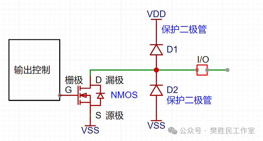
Figure 1 Open-drain output structure(Original image)
1. When the external load is powered by5V, the following circuit is generally used.
When driving an external load powered by 5V, the circuit shown in Figure 2 is commonly used. This circuit selects an I/O interface with 5V compatibility (FT), where the cathode of the internal protection diode D1 is connected to +5V instead of 3.3V, ensuring that even if an external +5V power supply is connected, D1 will not conduct due to forward bias, thus ensuring the safety of the interface.
The circuit operates as follows:
· When the internal control signal is high level, the NMOS transistor conducts, forming a current path: external +5V → resistor R and bulb → I/O pin → NMOS transistor drain-source → VSS (ground). At this time, the load is powered and operational.
· When the internal control signal is low level, the NMOS transistor is off, and the +5V power supply cannot form a current loop, causing the load to stop working.
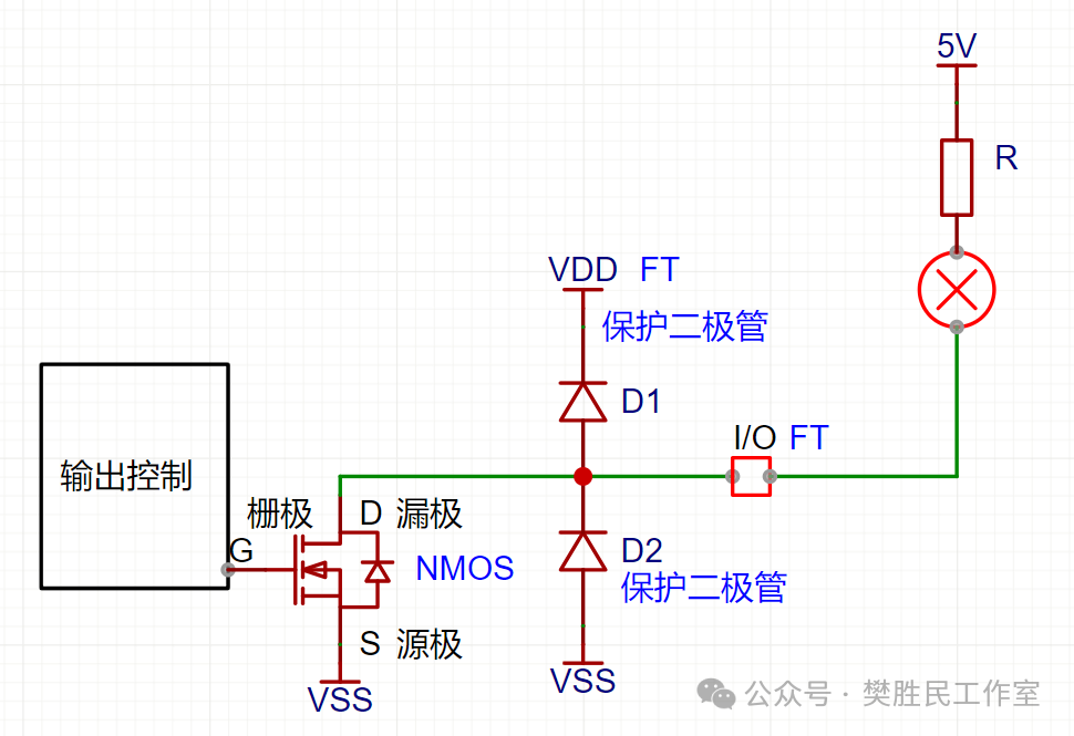
Figure 2(Original image)
2. When driving a circuit with a voltage higher than the chip voltage (5V), the following circuit is generally used.
To achieve stable high-level output, an external pull-up resistor must be connected to the power supply. When needing to drive a load with a working voltage higher than the chip voltage (such as 5V), the circuit structure shown in Figure 3 is typically used. The core of this design is to utilize open-drain output combined with an external pull-up resistor and driver device to safely control high-voltage loads with a low-voltage microcontroller.
Analysis of circuit working principle:
· When the internal control signal outputs high level, the NMOS transistor conducts, pulling the I/O port voltage down to near ground level. This low-level signal causes the external driving MOSFET to turn off due to insufficient gate voltage, breaking the load circuit and preventing the bulb from working.
· When the internal control signal outputs low level, the NMOS transistor is off, and the I/O port is in a high-impedance state. The external power VDD provides the driving voltage to the gate of the MOSFET through the pull-up resistor R, allowing it to fully conduct, thus forming a complete power supply circuit, and the bulb lights up normally.
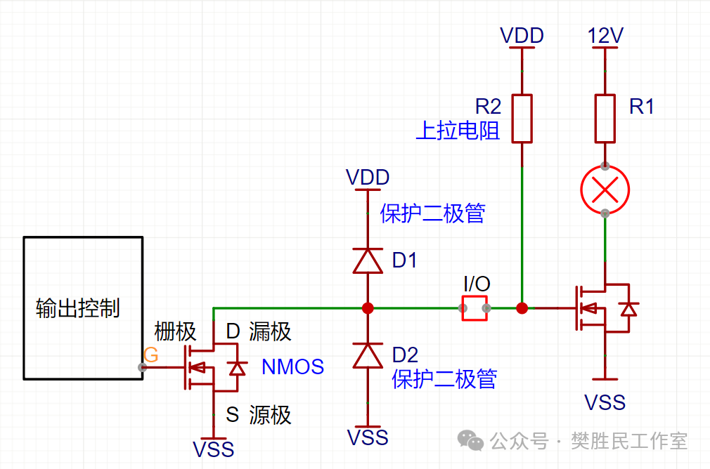
Figure 3 (Original image)
3. Achieving “Wired AND” Logic Safety
The core value of open-drain output lies in achieving multi-device bus sharing through “wired AND” logic safety. When multiple devices share a signal line, push-pull output can cause short-circuit risks due to level conflicts, while the open-drain architecture combined with a common pull-up resistor allows any device to pull the entire bus low when outputting a low level, and the bus is only pulled high when all devices output a high level. This hardware “wired AND” logic fundamentally avoids bus contention, becoming the circuit basis for bus protocols like I2C.
1
Thank you for enjoying my original article! This article is welcome to share, but to protect original rights, please indicate the source when reprinting. Thank you for your understanding!
2
Introduction: Fan Shengmin (186 3636 9649), member of the Yuncheng City Science Writers Association, member of the Shanxi Province Science Writers Association.Published “Playing with Electronics” in 2016, published “Super Fun Electronic Production” in 2017, published “Electrical Experiments in Life” in 2018, published “Arduino Programming and Hardware Implementation” in 2019, published “Introduction to Electronic Production” in 2021, published “Network Operation and Maintenance from Beginner to Pro” in 2022, published “Arduino Programming and Hardware Construction” in 2023, and will publish “Half-Hour Electronic Production” in 2025 and “Network Operation and Maintenance from Beginner to Pro” 2nd edition in 2025.