—–This articleIntroduction—–
Main content includes:
I2C Part One: Overview, Data Validity, Data Transmission, and Timing
Follow our WeChat official account:Hardware Learning Notes
Reply:Fan Group, to receive materials
—– Body —–
Like ↓ before reading, develop a habit!
1. Overview
I2C (Inter-Integrated Circuit) also known as IIC, is a serial communication protocol developed by Philips (now part of NXP Semiconductors), widely used to connect low-speed peripheral devices such as ADC, DAC, power management chips, current sensing chips, etc. It uses a two-wire system, supports a maximum communication frequency of 5MHz and supports multi-master and multi-slave modes.
2. Basic Structure
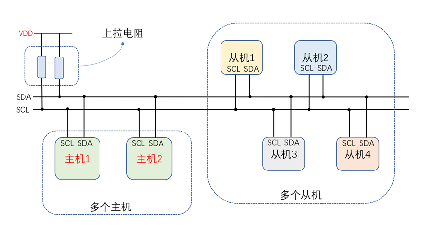
The basic structure of I2C is shown in the figure below, SCL and SDA are the communication buses, SCL: Clock Line, SDA: Data Line. Due to its arbitration feature, multiple masters and multiple slaves can be connected, and due to its open-drain output structure, both lines have pull-up resistors to provide a high level.
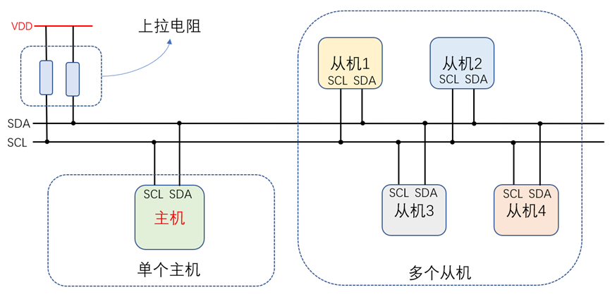
Of course, the most common usage is still single master and (single) multiple slaves:
3. Open-Drain Output and Logic
Open-Drain Output:
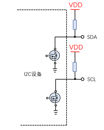
Open-drain output is a characteristic of I2C, meaning the output terminal connects to the external circuit through the MOS transistor’s drain, the source of the MOS transistor is grounded, and the gate is controlled. As shown in the figure below, this structure cannot output a high level; when the MOS transistor is turned on, it outputs a low level, and when the MOS transistor is turned off, it outputs a high-impedance state, meaning it neither pulls high nor pulls low. Therefore, an external pull-up resistor is needed to achieve a high level output.
One advantage of open-drain output is that even if various devices on the bus output high and low levels, since the high level is generated by the pull-up resistor, there will be no short circuit between VDD and GND on the bus.
Logic and Wiring:
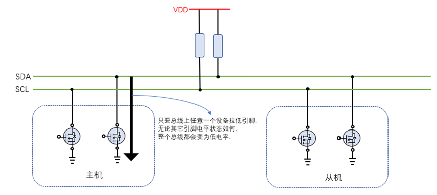
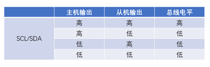
Wiring logic is similar to that of an AND gate; due to the open-drain output, as long as one device outputs a low level on the bus, the bus will be low, as shown in the table below:
4. Data Validity:
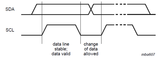
When I2C is transmitting data, the following logic must be followed to maintain data validity:
When SCL is high: The data on the SDA line must remain stable.
When SCL is low: The data on the SDA line can change.
5. Data Transmission:
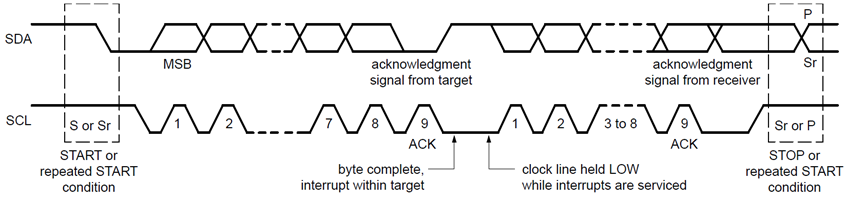
Below is a timing example provided by the official documentation
5.1 Bit Transmission:
From the timing diagram above, it can be seen that in I2C transmission, each 8 bits form a byte, followed by an acknowledgment or non-acknowledgment bit
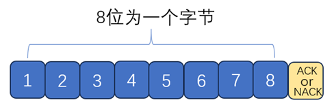
Acknowledgment Bit (ACK): The device pulls SDA low
Non-Acknowledgment Bit (NACK): SDA remains high
Additionally:
Read: SDA remains high
Write: The master pulls SDA low
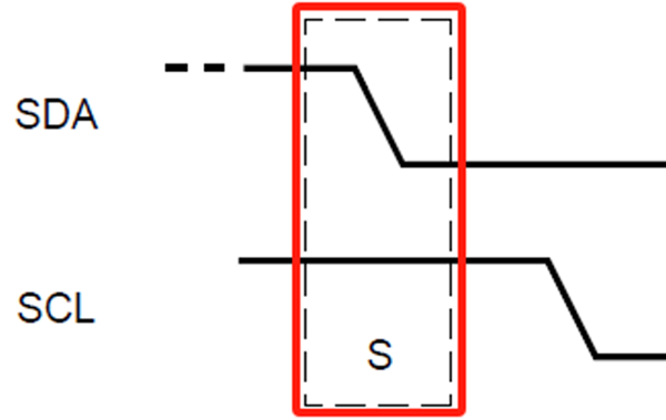
Start Bit: When SCL is high, SDA transitions from high to low.
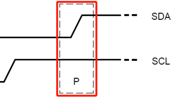
Stop Bit: When SCL is high, SDA transitions from low to high.
5.2 Common Timing
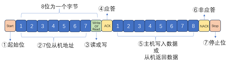
Below is an abstract diagram of the most common timing, which starts with ① Start Bit, then the master sends ② Seven-bit Slave Address, followed by ③ Read or Write Bit. After that, wait for the slave ④ Acknowledgment. After the slave acknowledges, ⑤ if reading data, the slave will return data for the master to read; if writing data, the master will write one bit of data. After reading or writing is complete, the master or slave will send ⑥ Non-Acknowledgment signal again, followed by sending ⑦ Stop Bit to stop this communication.
There is also a more complex common timing, which starts with ① Start Bit, then the master sends ② Seven-bit Slave Address, followed by ③ Write Bit. After that, wait for the slave ④ Acknowledgment. After the slave acknowledges, the master ⑤ Sends Register Address. After the slave receives it, it acknowledges again ⑥. After the master receives the acknowledgment, it sends ⑦ Start Bit again, and sends the Slave Address again, then sends Read or Write Bit. After that, wait for the slave 10. Acknowledgment. After the master receives the acknowledgment, 11. it sends data to the slave or reads data returned by the slave. After that, the master or slave sends 12. Non-Acknowledgment signal again, and finally the master sends Stop Bit to stop this communication.

The key to the above timing is The first byte sends the slave address, followed byThe second byte of the slave’s register address, The third byte sends the slave address again, and then The fourth byte is the data to be written or read. This timing is friendly for slightly more complex chip communications, as it allows configuration for different registers.
6. Actual Timing Example:
Below is a timing diagram for reading data, with the slave address: 1011 001, and the data returned by the slave: 0101 1101

Welcome to discuss in the comments section, don’t forget to like!!!

Click the lower left corner “Read Original”, materials, books, one-on-one introductory guidance, all available