The I²C (Inter-Integrated Circuit) protocol was developed by Philips Semiconductors (now NXP Semiconductors) and released in 1982. It is a serial, half-duplex bus primarily used for communication between chips over short distances at low speeds. The I²C bus consists of two bidirectional signal lines: one data line (SDA, serial data) for sending and receiving data, and one clock line (SCL, serial clock) for synchronizing the clocks of the communicating parties. The hardware structure of the I²C bus is simple and cost-effective, leading to its widespread application across various fields.
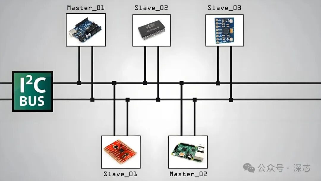
Main Features:
| Feature | Description |
|---|---|
| Physical Lines | 2: Serial Data Line (SDA) + Serial Clock Line (SCL) |
| Communication Direction | Half-duplex |
| Topology | Multi-master, multi-slave bus |
| Addressing Method | Software address addressing (7-bit or 10-bit address) |
| Speed Modes | Standard mode (100kbps), Fast mode (400kbps), High-speed mode (3.4Mbps), Ultra-fast mode (5Mbps) |
| Output Type | Open-drain output, requires external pull-up resistors |
| Notable Features | Simple hardware connection, low cost, supports multi-master arbitration and clock synchronization, has an acknowledgment mechanism |
| Typical Applications | Connecting sensors, memory (such as EEPROM), displays, real-time clocks (RTC), GPIO expansion chips, etc. |
Working Principle and Process:
In I²C bus communication, all devices are connected in parallel on the two lines. Each device has a unique address. Communication is initiated by the master, which controls the rhythm of the clock line SCL. Data is transmitted on the data line SDA.
A complete I²C data transmission resembles an orderly conversation, typically consisting of the following stages:
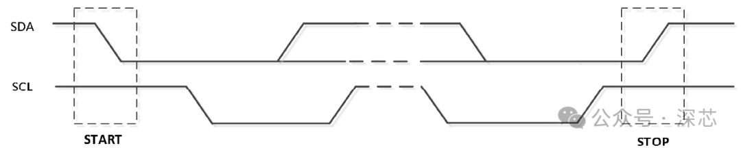
1. Start Condition: When SCL is high, the SDA line transitions from high to low. This falling edge informs all slaves that the bus is busy and to listen for the address.
2. Address Frame + R/W Bit: The master sends a 7-bit or 10-bit slave address, followed by a data direction bit (read/write bit). A 0 indicates the master wants to write data to the slave, while a 1 indicates the master wants to read data from the slave.
3. Acknowledgment Bit (ACK/NACK Bit): The slave that receives the address, if it recognizes its own address, should send an acknowledgment (ACK) signal by pulling SDA low during the next clock pulse. If it does not recognize (or cannot respond), SDA remains high, indicating a non-acknowledgment (NACK).
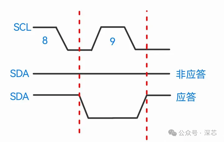
4. Data Frames: After receiving the address acknowledgment, data transmission begins. Each data frame consists of 8 bits, followed by an acknowledgment bit (ACK/NACK) to confirm successful reception. During data transmission, the most significant bit (MSB) is sent first.
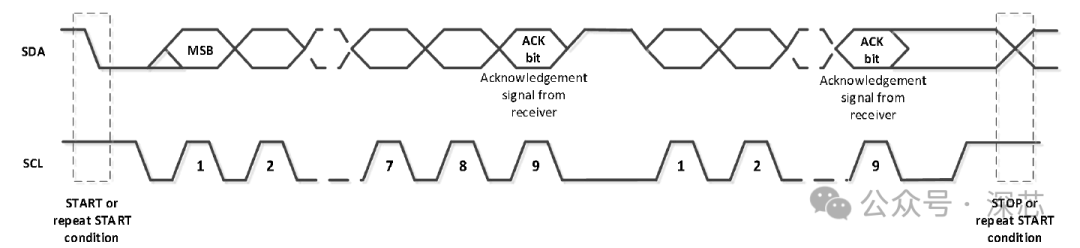
5. Stop Condition: Once all data transmission is complete, the master generates a stop condition. When SCL is high, the SDA line transitions from low to high. This rising edge indicates the end of communication, and the bus returns to idle.
Idle State: When I2C is idle, both SCL and SDA are high.
Data Validity:
A crucial rule in I2C communication is:
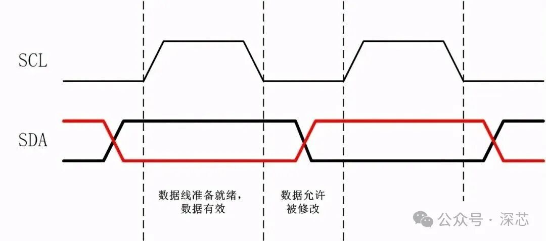
During the high state of SCL, the data on SDA must remain stable (no changes allowed) so that the receiver (whether master or slave) can accurately sample it.
During the low state of SCL, changes on the SDA line are allowed to prepare for the transmission of the next bit.
Slave Address:
In 7-bit address mode, the I2C protocol specifies that the high 7 bits of the address byte are the slave’s address, with the least significant bit being 0 for writing to the slave and 1 for reading from the slave.
In 10-bit address mode, the address consists of two bytes. When writing to the slave, the I2C protocol specifies: the first byte sends 11110XX0, with the high 5 bits fixed as 11110, bit2 and bit1 are the high 2 bits of the 10-bit address, and bit0 is the direction bit, with a value of 0 indicating a write direction; the second byte is the low 8 bits of the 10-bit address. When reading from the slave, the I2C protocol specifies: first send the write address (two bytes), then send the read address (the read address only requires sending one byte). The specific process is as follows: first send the write address, the first byte sends 11110XX0, with the high 5 bits fixed as 11110, bit2 and bit1 are the high 2 bits of the 10-bit address, and bit0 is the direction bit, with a value of 0 indicating a write direction; the second byte is the low 8 bits of the 10-bit address; then send the read address, sending 11110XX1, with bit2 and bit1 as the high 2 bits of the 10-bit address, and bit0 as the direction bit, with a value of 1 indicating a read direction.
Bus Arbitration:
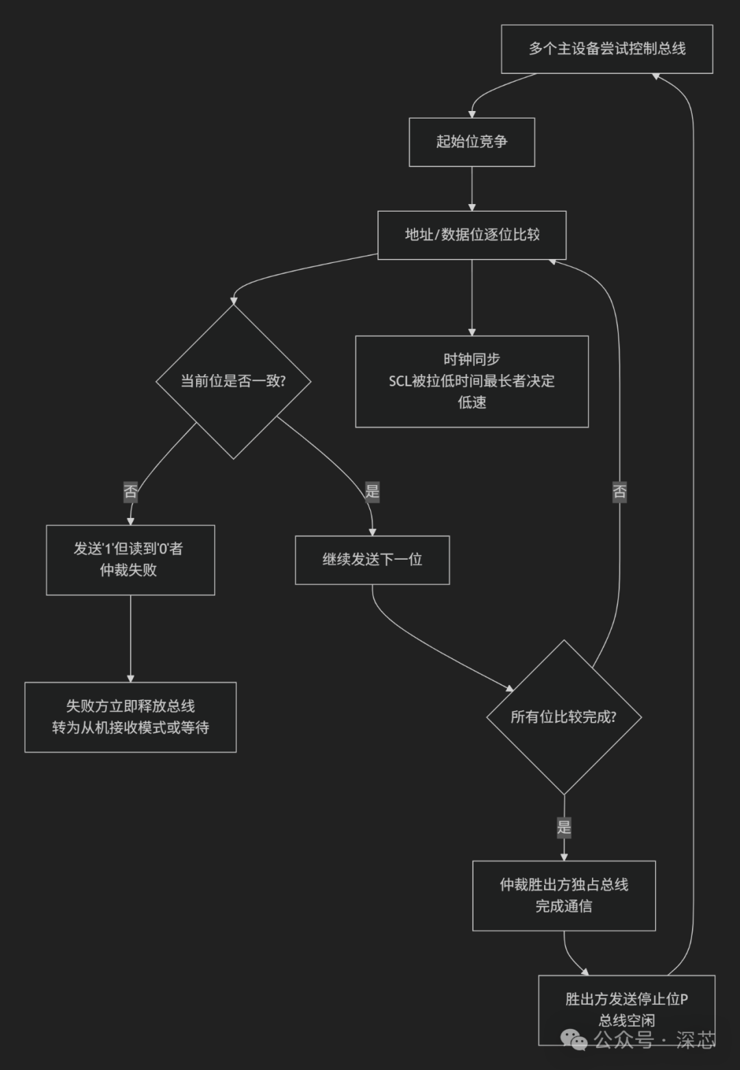
I²C supports multi-master operation.Bus arbitration is designed to resolve the issue of multiple devices competing for control of the bus. It determines which device can gain final control of the bus through a certain mechanism.The master checks the actual level on the SDA line after sending each bit. If it finds that it sent a 1 (released the bus), but the SDA line is low (pulled low by another master), then that master loses arbitration, exits the competition, and switches to slave mode. Arbitration starts comparing from the high bits of the address frame, and the master that can completely send the address wins the arbitration.
The clock synchronization mechanism allows multiple masters to generate their own clocks on the SCL line and collectively determine the final clock cycle through a “wired AND” logic, achieving synchronization.
(The SDA and SCL pins of I²C devices are both open-drain outputs. As long as one device outputs a low level, the bus is pulled low; the bus is high only when all devices output high (release the bus). This is the physical basis for arbitration.)
Beware of bus deadlock: If a device (especially a slave) malfunctions (e.g., program runaway, power failure) and continuously pulls the SDA line low, it will cause the entire bus to hang, interrupting all communication. Solutions include:
-
Software Reset: The master generates multiple SCL clock pulses (e.g., 9) to attempt to “wake up” the stuck slave device.
-
Hardware Reset: Reset the entire system or faulty device if necessary.
Pull-up Resistor Selection:
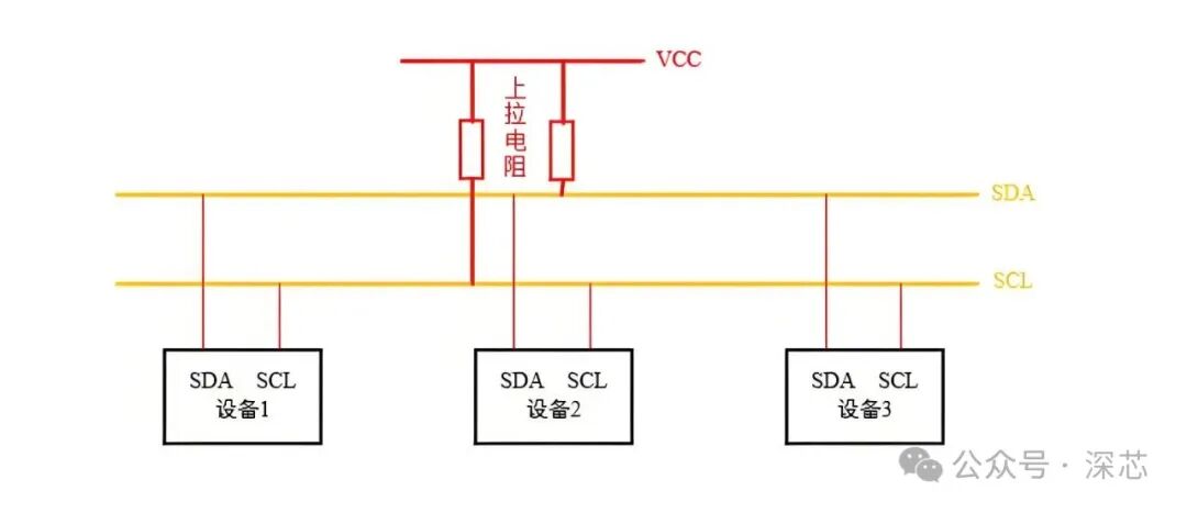
The I²C bus uses open-drain outputs, meaning devices can only pull the bus low (output low) and cannot drive it high directly. The high state of the bus needs to be pulled up to the supply voltage (VDD) by pull-up resistors (Rp). The value of Rp needs to be carefully calculated; too large or too small can lead to communication failure. Why pull-up resistors are needed on the I2C bus:
1. Calculate the minimum value Rp(min): Rp cannot be too small; otherwise, when the device tries to pull the bus low, the required sinking current (Iol) may exceed the device’s rated value, leading to an elevated low-level voltage (Vol) or even damaging the port. The formula is:
Rp(min) = (VDD – Vol(max)) / Iol
Where Vol(max) is the maximum low-level voltage allowed by the protocol (usually 0.4V or 0.3VDD), and Iol is the sinking current capability of the device (provided in the datasheet).
2. Calculate the maximum value Rp(max): Rp also cannot be too large; otherwise, the rise time (tr) of the bus’s load capacitance (Cb) through Rp will be too long, causing the signal edges to be too slow, which may not reach a reliable high level within the clock cycle at high baud rates. The formula is:
Rp(max) = tr / (0.8473 * Cb)
Where tr is the maximum rise time allowed in I²C mode (as per the datasheet or protocol specification), and Cb is the total capacitance of the bus.
3. Trade-offs and Selection: Choose a nominal value between Rp(min) and Rp(max). A smaller Rp (e.g., 1.5kΩ) can provide faster rise edges, suitable for higher speeds, but consumes more power; a larger Rp (e.g., 4.7kΩ or 10kΩ) consumes less power but limits the maximum communication rate.
PCB Layout and Wiring Specifications:
-
SDA and SCL signal lines should run parallel and of equal length, with a recommended width of 0.2-0.3mm, and a spacing greater than the line width to reduce crosstalk. Preferably routed on the surface layer and minimize total length.
-
Reduce branches: Devices should be concentrated in layout to avoid excessively long branches (stubs) on the bus, reducing signal reflection.
-
Pull-up resistor placement: Pull-up resistors should typically be placed near the main controller.