
Click the blue text to follow us

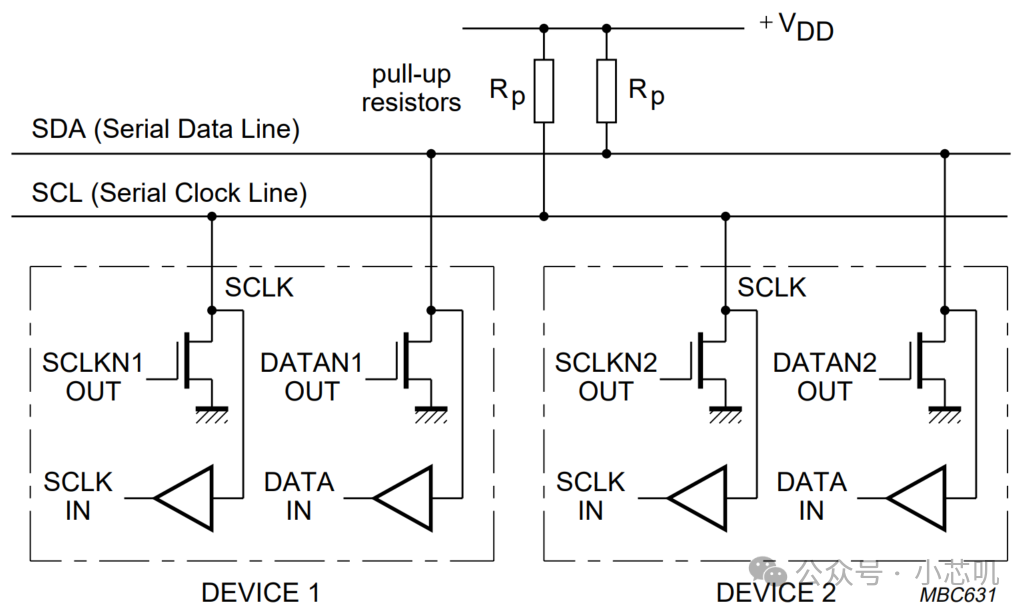
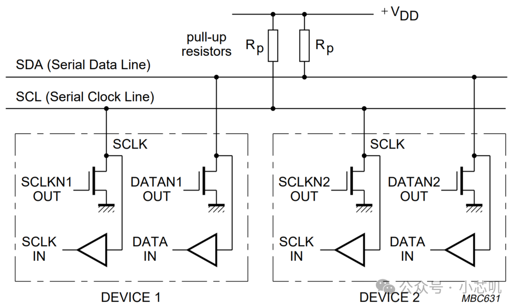
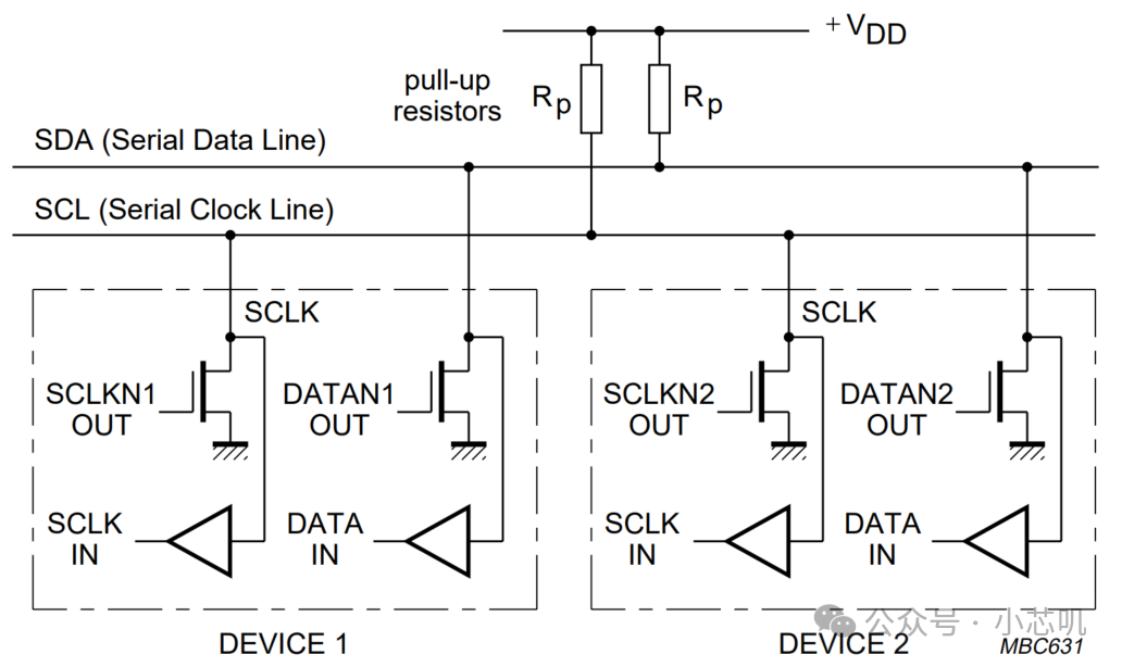
The I2C (Inter-Integrated Circuit) bus is a two-wire serial expansion bus introduced by Philips for connecting IC devices. Devices connected to the I2C bus can transmit data via the Serial Data Line (SDA) and Serial Clock Line (SCL).
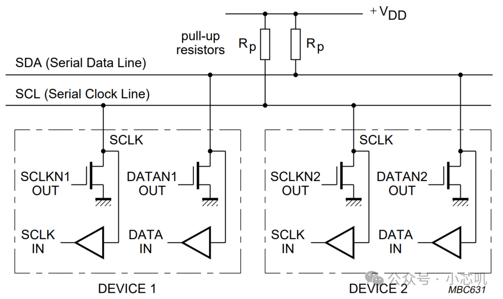
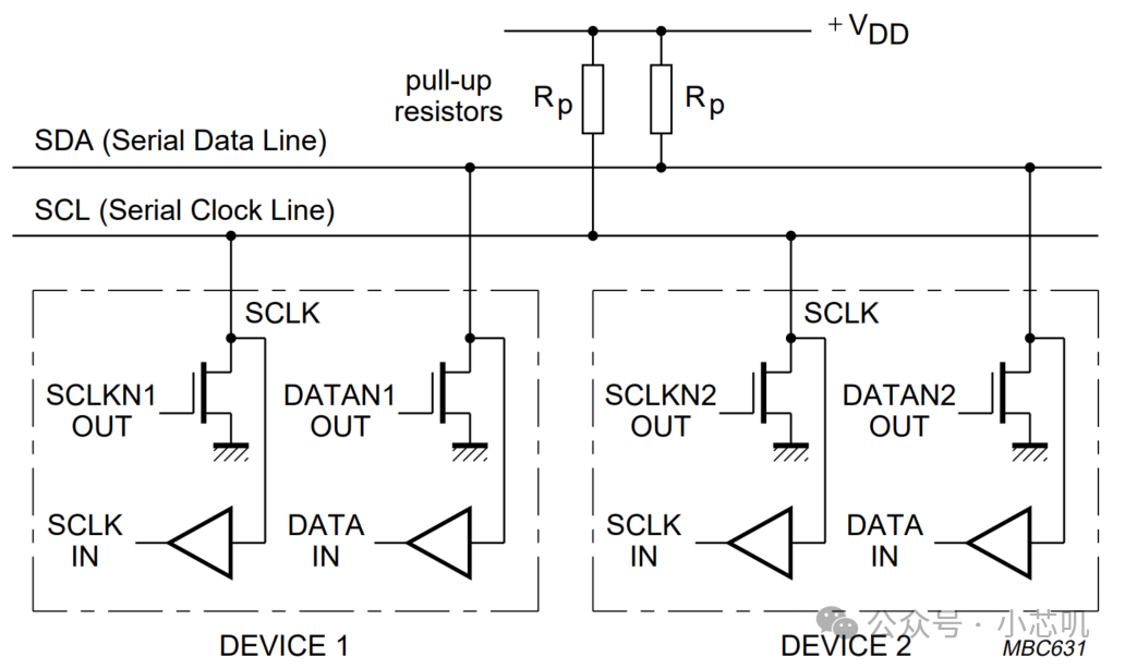
I2C Bus Structure
Both SCL and SDA of the I2C bus use open-drain or open-collector output methods, which have a “wired-AND” function. Thus, devices connected to the I2C bus can only pull SCL/SDA down to a low level and cannot force it up to a high level. Therefore, SCL and SDA must be pulled up to the positive power supply through pull-up resistors, and when the bus is idle, both lines are at a high level.
The resistance value of the pull-up resistor determines the communication rate of I2C; theoretically, the smaller the resistance, the higher the baud rate. Generally, when the communication speed is 100kbps, the pull-up resistor is set to 4.7kΩ; when the communication speed is 400kbps, the pull-up resistor is set to 1kΩ.
SDA is used to send data to the bus or receive data from the bus. The master sends the clock through SCL while also detecting the SCL level on the bus. The slave receives the SCL clock and sends or receives data on SDA under the control of SCL.
On the I2C bus, bidirectional serial data is transmitted in bytes, with five speed modes, and different devices can support different speeds.
-
Standard mode: 100kbps
-
Fast mode: 400kbps
-
Fast mode+: 1Mbps
-
High-speed mode: 3.4Mbps
-
Ultra-fast mode: 5Mbps (unidirectional transmission)
Communication is initiated by the master, which first sends the slave address; only the addressed slave can communicate with the master. During the address and data transmission process, the master generates the clock signal. If two or more masters start data transmission simultaneously, arbitration can prevent data corruption.The number of devices connected to the I2C bus is limited only by the total load capacitance on the signal lines; theoretically, any number of devices can be connected as long as the limit of 400pF is not exceeded.
Due to its fewer pins, simple hardware, ease of establishment, and strong scalability, I2C has gained recognition from many device manufacturers, with almost all mainstream manufacturers’ products, such as STMicroelectronics, Microchip, TI, and NXP, integrating the I2C serial bus.
Data Transmission on the I2C Bus
1
Input and Output Voltage Levels
For each data bit transmitted, the master generates a clock pulse. Since the devices connected to the I2C bus vary, the logic 0 (low) and logic 1 (high) levels are not fixed but depend on the relevant level of +VDD.
2
Data Validity
During data transmission on the I2C bus, the data on SDA must remain stable while the SCL signal is high. Only when the SCL signal is low can the data on SDA change.
I2C Data Validity
3
START and STOP Conditions
START and STOP conditions are generated by the I2C master.
-
START Condition is defined as the SDA line transitioning from high to low when SCL is high. The master drives this condition to indicate the start of data transmission. After the START condition, the bus is considered busy.
-
STOP Condition is defined as the SDA line transitioning from low to high when SCL is high. The master drives this condition to indicate the end of data transmission. After the STOP condition, the bus is considered idle.
START and STOP Conditions
4
Byte Format
During data transmission on the I2C bus, the data transmitted on SDA is in bytes, with the most significant bit (MSB) transmitted first. After sending one byte, the receiver must return an acknowledgment signal (Acknowledge Bit, ACK).The ACK width is 1 bit, immediately following the 8 data bits, so sending 1 byte of data requires 9 SCL clock pulses.If the slave is performing other tasks and cannot receive or send the next complete data byte, it can pull the clock line SCL low, causing the master to enter a wait state. When the slave is ready, it releases SCL to continue data transmission with the master.
I2C Byte Transmission and Acknowledgment
5
Acknowledgment Bit
Each data byte transmission must have an acknowledgment bit. The clock for the acknowledgment bit is generated by the master.During this clock cycle, the sender releases SDA, and the receiver pulls SDA low,producing an acknowledgment (ACK).
If the receiver does not pull SDA low during the ACK clock cycle, and SDA remains high during the acknowledgment bit clock cycle, it produces a no acknowledgment (NACK).
I2C Acknowledgment Bit
Below are several situations that can produce a NACK:
-
Slave does not acknowledge Slave Address: When the address does not match or the slave is performing other tasks and cannot timely receive or send data, it produces a NACK and does not acknowledge the master’s Slave Address.
-
Slave-Receiver does not acknowledge data byte: After receiving a segment of data, the slave may not be able to continue receiving further data for some reason. In this case, the slave produces a NACK after receiving the last data.
-
Master-Receiver does not acknowledge data byte: After the master receives the last byte, it must send a NACK. The slave will release SDA upon receiving the NACK, allowing the master to continue subsequent operations.
Upon receiving a NACK, the master can generate a STOP condition to terminate the transmission or generate a RESTART condition to start a new transmission.
Through this article, everyone has gained an in-depth understanding of the structure, basic characteristics, and data transmission rules of the I2C bus. In the next article, we will continue to introduce the I2C bus’s addressing format and four operating modes.
Thank you for reading my article. If you find it useful, please give me a follow! We will continue our discussion next time.
>/ Author: Xiao Xin Ji