The FPGA discussed here is a type of reprogrammable integrated circuit that enables customizable digital logic design, providing designers and engineers with a rapid prototyping platform for building complex, efficient, and innovative digital electronic solutions.
Introduction
Field-Programmable Gate Arrays (FPGAs) have become a versatile and powerful technology that allows engineers to create customized, reconfigurable digital circuits. With their unique flexibility, parallel processing capabilities, and rapid prototyping advantages, FPGAs are widely used in various industries, including communications, aerospace, and automotive.
This article aims to help you grasp the fundamentals of FPGA design, the design process, various application scenarios, and best practices for achieving efficient, high-quality designs. By the end of this article, you will have a solid foundation in FPGA system design, enabling you to fully leverage the potential of this outstanding technology in your projects.
Understanding FPGA Fundamentals
In this section, we will delve into the fundamentals of Field-Programmable Gate Arrays (FPGAs), including their main components, advantages, and comparisons with other technologies such as Application-Specific Integrated Circuits (ASICs) and microcontrollers.
What is an FPGA?
A Field-Programmable Gate Array (FPGA) is a semiconductor device that can be programmed and reprogrammed after manufacturing to implement various digital logic functions. FPGAs provide a unique approach to digital circuit implementation by offering programmable hardware modules and interconnection resources that can be flexibly configured to perform a wide range of tasks.
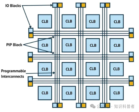
Components of an FPGA
Field-Programmable Gate Arrays (FPGAs) consist of several key components that work together to implement and configure customized digital circuits. The main components of an FPGA include:
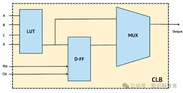
Configurable Logic Blocks (CLBs): These are the basic building blocks of an FPGA, containing Look-Up Tables (LUTs), flip-flops, and sometimes dedicated arithmetic units. CLBs can be configured to perform various combinational and sequential logic functions.
Programmable Interconnect Points (PIPs): These are programmable switches and wiring resources used to connect CLBs within the FPGA to other components. PIPs provide flexible signal routing and interconnection capabilities, allowing efficient communication between different elements on the chip. At a fundamental level, transistors are the basic building blocks of FPGAs, forming CLBs and PIPs.
Input/Output Blocks (IOBs): These serve as the interface between the FPGA and external devices or other components on the circuit board. IOBs can be configured to support various signal standards and communication protocols, enabling the FPGA to communicate with a wide range of peripherals.
Block RAM (BRAM): This is embedded memory on the FPGA chip used for data storage and various storage functions. Compared to off-chip memory, BRAM is faster and has lower access latency.
Digital Signal Processing Blocks (DSP Blocks): These are hardware modules specifically designed for high-speed arithmetic operations, such as multiplication and accumulation. DSP blocks are widely used in signal processing and filtering applications.
Clock Management Resources: This includes Phase-Locked Loops (PLLs) and Digital Clock Managers (DCMs) used to generate, distribute, and manage clock signals within the FPGA. These resources help maintain precise timing and synchronization throughout the device.
Configuration Memory: This is a type of flash memory used to store the configuration bitstream. This bitstream is used to program the FPGA to implement the desired digital circuit. Upon startup or when reprogramming is needed, this bitstream is loaded into the chip.
Traditionally, code is written and compiled into instructions that run on a processor. However, for FPGAs, code can be written in a hardware description language (HDL) in a different manner. This code is then synthesized into actual hardware modules and directly configured on the FPGA to perform the desired logic functions. These hardware modules in an FPGA consist of registers and various types of logic gates, such as AND gates, OR gates, NOR gates, NOT gates, XOR gates, and XNOR gates. These logic gates can be combined to construct complex digital circuits.
The key to FPGA flexibility lies in using Look-Up Tables (LUTs) to implement logic gate functions. Additionally, the interconnections between these logic blocks are also programmable, supporting flexible signal routing. By designing LUTs as programmable structures and utilizing a reconfigurable switching fabric to connect them, FPGAs can be customized to perform a wide variety of tasks. This is why FPGAs can run any logic required by the user as a single device, making them popular across various application domains, from prototyping to high-performance computing.
HDL Languages: VHDL and Verilog
Hardware Description Languages (HDLs) are used to describe digital circuits at a higher abstraction level. In FPGA design, the two mainstream HDLs are VHDL and Verilog.
VHDL: VHDL (VHSIC Hardware Description Language) is a strongly typed, verbose language with a high level of abstraction, making it easier to write complex designs. It is widely used in Europe and in industries such as aerospace and defense.
Verilog: Verilog is a more concise HDL similar to the C language, popular in the United States and commercial sectors. Compared to VHDL, it has a lower level of abstraction, which may present challenges when handling complex designs, but it also provides designers with finer control over hardware implementation.
Both languages have their pros and cons, and the choice between VHDL and Verilog often depends on personal preference or industry standards.
To better understand the differences between the two, let’s look at a piece of Python code that implements addition:
# python-add-numbers
def add_numbers(a, b):
    return a + b
In Python, this code is written in a high-level language that completely abstracts the underlying hardware details. The function <span>add_numbers</span> takes two input parameters <span>a</span> and <span>b</span> and returns their sum. This code is executed sequentially by the processor, with the CPU performing the addition operation.
Now, let’s look at a simple Verilog adder code:
// verilog-add-two-numbers
module Adder(
    input  [3:0] A,
    input  [3:0] B,
    output [3:0] Sum
);
    assign Sum = A + B;
endmodule
In this Verilog code, we define a module named <span>Adder</span> that includes two 4-bit input signals <span>A</span> and <span>B</span>, as well as a 4-bit output signal <span>Sum</span>. The code describes the behavior of a digital circuit through the <span>assign</span> statement—this circuit directly implements the addition of two numbers on the programmable logic resources of the FPGA, generating a custom hardware circuit specifically for 4-bit addition.
The core difference between these two methods is that the Python code is executed sequentially by the processor, while the Verilog code describes a digital circuit implemented directly in FPGA hardware. This means that the FPGA-based adder can perform addition operations in parallel, typically faster than the processor running the Python code. However, Python offers advantages in flexibility and ease of use, while Verilog requires designers to have a deeper understanding of digital circuit design and FPGA resources.
Advantages of FPGAs
Compared to other technologies, FPGAs offer several advantages:
- Flexibility: FPGAs can be reprogrammed to achieve different functionalities, suitable for a wide range of applications.
- Rapid Prototyping: FPGAs enable designers to quickly test and iterate design solutions, reducing time to market.
- Parallelism: FPGAs can execute multiple tasks simultaneously, significantly enhancing performance in certain applications.
- Customization: FPGAs support the creation of application-specific hardware optimized for specific needs, often resulting in better performance and lower power consumption.
- In-field Reconfigurability: FPGAs can be reconfigured after deployment, allowing for functionality updates, bug fixes, or new features without replacing the entire hardware.
- Lower Non-Recurring Engineering (NRE) Costs: Compared to custom ASICs, FPGA development does not require high NRE costs, making them more suitable for small-scale production or proof-of-concept projects.
- Scalability: FPGA designs can be easily scaled up or down based on demand, achieving efficient resource utilization and cost-effective solutions.
- Security: FPGAs can provide higher security through hardware-based encryption and secure boot features, making them harder to tamper with compared to pure software implementations.
- Analog and Digital Interface Capabilities: FPGAs can interface with various analog and digital peripherals, simplifying system integration and enabling seamless communication between different components.
- Long Lifecycle: FPGA-based designs typically have a longer lifespan than ASICs, as they can adapt to evolving standards and technologies through updates and reprogramming.
- Design Reusability: IP cores and existing FPGA designs can be easily reused in new projects, significantly reducing development time and effort.
Disadvantages of FPGAs
Compared to other technologies such as ASICs and microcontrollers, FPGAs also have some drawbacks, including:
- Cost: For high-volume production, the unit cost of FPGAs is typically higher than that of microcontrollers or ASICs, making them less economical in high-yield scenarios.
- Power Consumption: FPGAs generally consume more power than ASICs and microcontrollers, which can become a bottleneck in power-sensitive applications.
- Design Complexity: The design process for FPGAs is more complex than for microcontrollers, requiring knowledge of hardware design, HDL programming, synthesis, and place-and-route tools.
- Performance Limitations: Although FPGAs have parallel processing capabilities and excel in certain tasks, they may still not outperform ASICs that are highly optimized for specific functions in certain applications.
- Chip Size: Due to the inclusion of many additional resources for programmability and reconfigurability, FPGAs are typically larger in physical size than equivalent-function ASICs or microcontrollers.
- Configuration Time: FPGAs require loading a configuration bitstream upon power-up, resulting in longer startup times compared to ASICs and microcontrollers.
FPGA vs. ASIC vs. PLD vs. Microcontrollers
FPGAs, Application-Specific Integrated Circuits (ASICs), Programmable Logic Devices (PLDs), and microcontrollers can all be used to implement digital logic functions, but they differ in several aspects. Here is a comparison of these technologies:
- FPGA: As mentioned earlier, FPGAs have reprogrammable features, suitable for a wide range of applications. They offer high performance and parallel processing capabilities but are generally more expensive and power-hungry than ASICs, PLDs, and microcontrollers.
- ASIC: ASICs are chips customized for specific applications, offering optimized performance and power characteristics. However, they require high upfront investment, long development cycles, and lack the flexibility of FPGAs and PLDs, making them more suitable for mass production.
- PLD: Including Complex Programmable Logic Devices (CPLDs) and Simple Programmable Logic Devices (SPLDs), PLDs are similar to FPGAs but have simpler structures and fewer resources. They are suitable for simpler digital designs, typically at lower cost and power than FPGAs, but may lack sufficient performance and flexibility in complex applications.
- Microcontrollers: Microcontrollers are general-purpose computing devices that integrate memory, processors, and input/output functions. They are usually slower than FPGAs and PLDs and do not have parallel processing capabilities, but they are low-cost, low-power, and have a low development barrier.
In summary:
- FPGAs offer flexibility and parallelism;
- ASICs achieve extreme optimization in performance and power;
- PLDs emphasize simplicity and cost-effectiveness;
- Microcontrollers excel in low cost and ease of development.
Technology selection should be based on specific application requirements, balancing performance, power consumption, development time, and cost.
FPGA Design Process and Methodology
This section will introduce the complete design process for FPGAs, including an overview of the design process, hardware description languages, Register Transfer Level (RTL) design, synthesis, implementation, and testing and debugging.
Overview of the Design Process
The FPGA design process consists of several steps that guide designers from concept to a fully functional FPGA implementation. The main steps are as follows:
- Design Entry: Designers use hardware description languages (HDLs) such as VHDL or Verilog to write a high-level description of the target digital circuit.
- RTL Design and Simulation: The HDL code is converted into Register Transfer Level (RTL) representation and verified for functionality and performance through simulation.
- Synthesis: The RTL design is transformed into a gate-level netlist, which is a circuit representation composed of logic gates and flip-flops.
- Implementation: The gate-level netlist is mapped to the physical resources of the FPGA, including Configurable Logic Blocks (CLBs), DSP slices, and programmable interconnects. This stage includes place-and-route and bitstream generation.
- Testing and Debugging: The FPGA device is tested and debugged using simulation tools, testbenches, or target hardware to ensure its functionality and performance requirements are met.
Throughout the design process, various tools and software are used to facilitate the design, simulation, synthesis, and implementation of FPGAs.
RTL Design and Simulation
RTL (Register Transfer Level) design is an intermediate representation of digital circuits that focuses on the flow of data between registers and the operations performed on that data. RTL simulation is used to verify the functionality and performance of the design before entering the synthesis and implementation stages. Common RTL simulation tools include ModelSim, XSIM, and VCS. These tools allow designers to perform functional and timing simulations, helping to identify and correct design errors and performance bottlenecks early in the design process.
Synthesis and Implementation
During the synthesis stage, the RTL design is converted into a gate-level netlist, which represents the digital circuit using logic gates and flip-flops. This process involves optimizing the design for area, speed, and power consumption. Common synthesis tools include Xilinx Vivado, Intel Quartus, and Synopsys Design Compiler. The implementation stage involves mapping the gate-level netlist to the FPGA’s resources, such as CLBs, DSP slices, and programmable interconnects. This step includes place-and-route (determining the physical locations of design elements on the FPGA) and bitstream generation (creating the binary file used to configure the FPGA). Implementation tools include Xilinx Vivado and Intel Quartus. EDA (Electronic Design Automation) tools play a crucial role in the FPGA design process, assisting designers in completing all tasks from synthesis, layout, routing, to verification.
Testing and Debugging FPGA Designs
Testing and debugging are critical steps in the FPGA design process, ensuring that the design operates correctly and meets performance requirements. Common testing methods include:
- Simulation: Testing the design in a virtual environment using simulation tools, allowing for faster and more controllable testing.
- In-circuit Testing: Testing the FPGA design on a test platform or target hardware, typically using logic analyzers or oscilloscopes to monitor signals and identify issues.
Debugging FPGA designs involves identifying and resolving issues related to functionality, performance, and resource utilization. Best practices include: using descriptive signal and variable names to improve code readability; adopting a modular design approach to break the design into smaller, more manageable components; and utilizing simulation tools and in-circuit testing to identify and isolate problems. By following the FPGA design process and adopting best practices for testing and debugging, designers can create high-quality FPGA designs that meet specific application requirements.
FPGA Design Examples and Applications
This section will explore various examples and applications of FPGA designs.
Using FPGAs for Digital Signal Processing (DSP)
DSP is the process of manipulating and analyzing digital signals such as audio, video, or sensor data. Due to their parallel processing capabilities and flexibility, FPGAs are well-suited for DSP tasks. Some FPGA-based DSP application examples include audio processing (e.g., audio effects, equalization, noise reduction, and compression), image processing (such as real-time edge detection, filtering, and object recognition), and software-defined radio (SDR) for implementing various radio communication protocols, making radio systems highly customizable and adaptable.
FPGA-based Artificial Intelligence (AI) and Machine Learning (ML)
FPGAs play a significant role in AI and ML applications, providing low latency, high throughput, and energy efficiency advantages. Some FPGA-based machine learning and AI project examples include deep learning accelerators, edge AI computing, and custom AI hardware implementations to optimize performance and energy efficiency for specific applications.
FPGA Applications in Networking and Communications
FPGAs are widely used in networking and communication systems, offering high performance, flexibility, and adaptability. Examples of FPGA-based networking and communication projects include implementations of high-speed Ethernet switches and routers, high-speed data transmission and signal processing in optical communication systems (such as Dense Wavelength Division Multiplexing, DWDM), and implementations of wireless communication protocols (such as 5G, Wi-Fi, and Bluetooth).
In summary, FPGAs are versatile and powerful devices that can be widely applied in various fields, from digital signal processing and machine learning to network communications—where the capabilities of microprocessors often exceed actual needs. By fully leveraging the unique advantages of FPGAs, designers can develop innovative and high-performance solutions for various industries and application scenarios.
Best Practices for FPGA Design
This section will discuss general best practices for FPGA design, focusing on code readability, modular design, and techniques for optimizing performance, power consumption, and resource utilization.
Code Readability and Modularity
Maintaining code readability and modularity is crucial for efficient FPGA design. Following these practices can enhance the maintainability and scalability of the design:
- Descriptive Naming: Use meaningful names for signals, variables, and modules to make the code easier to understand.
- Add Comments: Use comments to explain the purpose and functionality of the code, especially for complex or non-intuitive operations.
- Modular Design: Break the overall design into smaller, more manageable modules or components. This approach facilitates debugging, maintenance, and code reuse.
FPGA Design Optimization for Performance, Power, and Resource Utilization
Optimizing FPGA designs helps achieve an ideal balance between performance, power consumption, and resource usage. Common optimization techniques include:
- Pipelining: Break complex operations into multiple stages for parallel processing to increase throughput and reduce latency.
- Resource Sharing: Reuse hardware resources (such as multipliers, converters, or storage blocks) among multiple operations to save area and power.
- Clock Gating: Disable clock signals for unused or idle parts of the design to reduce dynamic power consumption.
In addition to the above methods, make full use of the optimization features provided by synthesis and implementation tools (such as Xilinx Vivado and Intel Quartus). These tools can help you achieve the best results based on your specific design requirements and constraints.
By following best practices for FPGA design and applying optimization techniques, you can develop high-quality, efficient designs that fully meet the requirements of specific applications.
Conclusion
In this article, we explored the fundamentals of FPGA design, the design process, various application scenarios, and best practices for creating efficient, high-quality designs. By gaining a deeper understanding of how FPGAs work and fully leveraging their unique capabilities, designers can create innovative solutions for numerous industries and application scenarios.
As you embark on your FPGA design journey, keep in mind the best practices outlined in this article, choose the right FPGA for your projects, and continuously refine your design skills.
Frequently Asked Questions (FAQ)
Q: What are the main advantages of using FPGAs?A: FPGAs offer flexibility, reprogrammability, parallel processing capabilities, and rapid prototyping capabilities, making them suitable for a wide range of applications.
Q: How do I choose the right FPGA for my project?A: When selecting an FPGA, consider factors such as device series, manufacturer, resource requirements, performance specifications, and cost.
Q: Can FPGAs be used for machine learning and artificial intelligence applications?A: Yes. FPGAs have advantages in AI/ML applications due to their low latency, high throughput, and energy efficiency.
Q: What are the differences between VHDL and Verilog?A: VHDL is a strongly typed, verbose language with a higher level of abstraction; Verilog is more concise, similar to C language, with a lower level of abstraction. The choice of language often depends on personal preference or industry standards.
Q: What tools and software do I need to start FPGA design?A: You will need an HDL editor, simulation tools (such as ModelSim, XSIM), synthesis tools (such as Xilinx Vivado, Intel Quartus), and implementation tools (also Vivado or Quartus).