Source: Content from “Mo Shang Feng Qi Lu Kan IC“, Author: Mo Shang Feng Qi Lu, thank you..
With support from various parties, integrated circuits have become a hot topic of the era, and there are numerous articles discussing the complexity and difficulties of chip design. I plan to clarify the chip design process from the perspective of EDA usage. After drawing the first diagram, I found that I was only familiar with a small part of the digital circuit section, completely ignorant of the system, software, and upper-level applications, so I can only categorize this as Others.
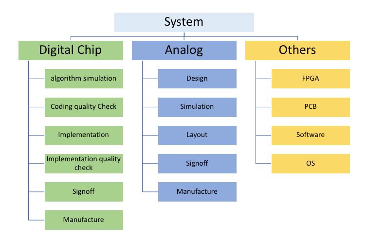
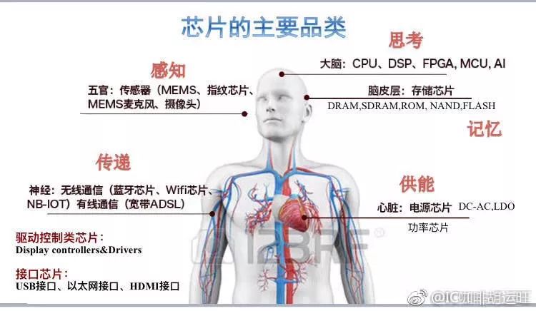
For consumers, a usable system consists of a digital integrated circuit part, an analog integrated circuit part, system software, and upper-level application parts. The functions of each part can be clearly understood by referring to the exquisite diagram from IC Coffee’s Hu Zong. The external world is an analog world, so all parts that need to interface with the external world require analog integrated circuits. The analog integrated circuit converts the external information collected into 0/1 for processing by the digital integrated circuit, and then converts the processed signal back into an analog signal for output; and this entire computation process is completed under the command and supervision of system software, hence it is said: the chip is the skeleton, and the system software is the soul.
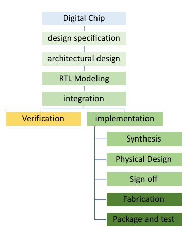
The design implementation process of digital integrated circuits is quite lengthy. Taking mobile baseband chips as an example, for 3G, 4G, and 5G, engineers initially encounter countless pages of protocol documents. Architects must determine based on the protocols: which parts of the protocol can be implemented in software and which parts need to be implemented in hardware; algorithm engineers must study every part of the protocol in depth and select the algorithms to be used for implementation; chip design engineers need to describe the algorithms selected by the algorithm engineers in RTL; chip verification engineers need to design test vectors based on the algorithms selected by the algorithm engineers to verify the functionality and performance of the RTL; digital implementation engineers need to transform the RTL into GDS based on the target PPA set by the algorithm and design engineers; due to the complexity of chip production, it is entirely handed over to foundries, and packaging is also done by them; for testing, most companies rent third-party testing platforms for their own testing engineers to complete, with only a few wealthy companies having their own testing platforms.
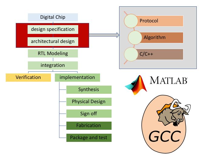
A chip’s performance is 60% dependent on the architect. In China, there are no more than a hundred good architects, and no more than ten excellent architects. Architects are the creators of the chip’s soul, at the top of the food chain, and a brilliant existence. From my limited understanding, besides office tools, it seems there are no EDA tools for architectural design; once the architecture is determined, a large number of algorithm engineers follow suit. For every point specified by the protocol, a suitable algorithm must be selected, and precise simulations must be performed using C/C++ to ensure functionality, accuracy, efficiency, and throughput metrics. Matlab and GCC should be the most frequently used tools by them.
Design engineers convert the algorithms selected by the algorithm engineers through repeated simulations and verifications into RTL. During the design process, they need to repeatedly simulate and synthesize to confirm the correctness of the design functions and the achievable PPA. Besides RTL, design engineers also need to write SDC and power intent based on the design goals and perform corresponding quality checks.Design engineers need to use a large number of EDA tools:
-
Editors: VIM, emac;
-
Lint: RTL quality checks, Spyglass, Jasper;
-
CDC: SDC quality checks, Spyglass, Conformal, GCA;
-
CPF/1801: power intent quality checks, CLP;
-
Power: RTL level power analysis, Joules, PA;
-
Simulators: C, S, M each have their own simulation tools;
-
Synthesis: Genus, DC;
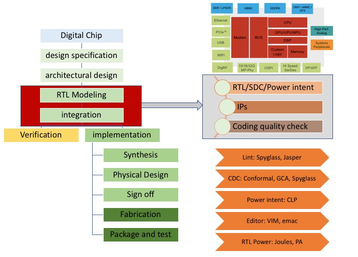
I believe that from integration, the transition from mental labor to physical labor is like moving from a designer to a bricklayer. Integration engineers need to connect all the modules used by the chip together, guided by the philosophy determined by the architecture engineer, while how each IP connects is determined by the owner of each IP. The integration engineer only needs to ensure that there are no extra, missing, or incorrect connections. It is said that there are currently no effective integration tools, and the commonly used one is emac.
Verification
Next, in actual projects, verification and synthesis will begin to overlap from RTL coding and iterate repeatedly.
Verification occupies a large proportion in digital chip design. In recent years, driven by the complexity of design, verification methodologies and means have been continuously updated, from OVM to UVM, from dynamic verification to static verification, from FPGA to emulator. All innovations can be summarized as: fast, complete, and easy to debug. Verification involves many aspects. Verification engineers must have sufficient understanding of the relevant protocol algorithms and design simulation vectors based on the goals set by architects and algorithm engineers; on the other hand, they must have sufficient understanding of the design itself to improve verification efficiency and shorten verification time.Verification engineers need to master many technologies and use many tools.
-
Languages: besides various scripting languages, C/C++, SystemVerilog, Verilog;
-
Protocols: various interface protocols, various communication protocols, various bus protocols;
-
Tools: dynamic simulation tools, static simulation tools, FPGA, emulator;
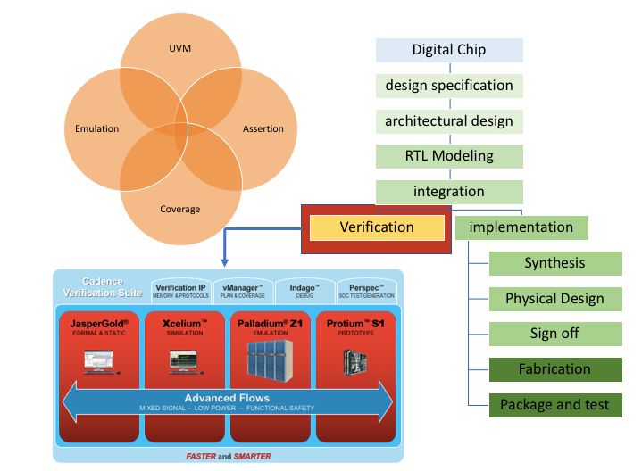
In the field of digital verification, C, S, and M almost completely dominate. I haven’t done verification for many years and have almost no knowledge of S and M’s verification-related tools except for VCS, Verdi, and Modelsim. Here, I will take C’s complete verification suite as an example.
-
Static Verification: Jasper Gold is a newly launched static verification tool from C. My understanding of static verification is that it is a verification methodology based on assertions, meaning static does not require input test stimuli; the verification process is a purely mathematical behavior.
-
Dynamic Verification: Xcelium is C’s dynamic verification tool. My understanding of dynamic verification is that it is a verification methodology based on UVM, where test stimuli are input, simulation results are monitored, and coverage is analyzed to complete functional verification.
-
Emulator: A hardware simulation accelerator, roughly understood as: a giant programmable array with debugging capabilities and rich interfaces; Features: ultra-fast verification, supports system software debugging. Palladium is C’s star product in the verification field, a leader in the industry. It is said that there are often inspections from high-ranking officials at silicon factories, lingering in front of Palladium, admiring its beautiful appearance and praising its powerful functions.
-
Verification IP: Verification requires various verification models, various IPs, various buses, and various high-speed interfaces.

One major application of FPGA is verification, so it’s worth mentioning. There were once two outstanding FPGA companies in the world, one was Altera and the other was Xilinx. Later, Altera, like Mentor, found a big company to sell itself. Besides programmable logic, FPGAs typically integrate various IPs, such as CPUs, DSPs, DDR controllers, etc. Each FPGA has various configurations, and depending on the integrated IPs and the scale of programmable logic, the price can vary greatly. Compared to ASICs, FPGAs also have a corresponding set of EDA tools for synthesis, layout, routing, programming, and debugging. For example: Synplify, Quartus.
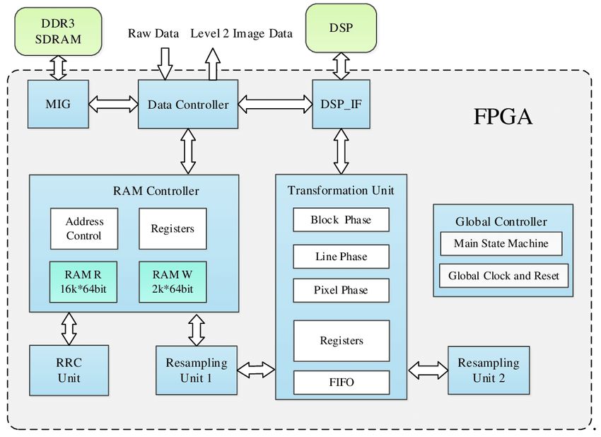
Current situation in China: Static Verification, Dynamic Verification, Emulator are almost blank; there are some FPGA companies in China that have done very well in the mid to low-end fields, but there is almost a blank space in the high-end field. There is a long way to go; no embellishments, just solid work!

Implementation
Continuing from what was mentioned earlier, we will continue to clarify the digital chip design implementation process, entering the implementation phase today. For this part, I am only familiar with synthesis, formal verification, low-power verification, RTL power analysis, STA; other parts are only vaguely understood, so I will not delve deeper, just clarify the process.
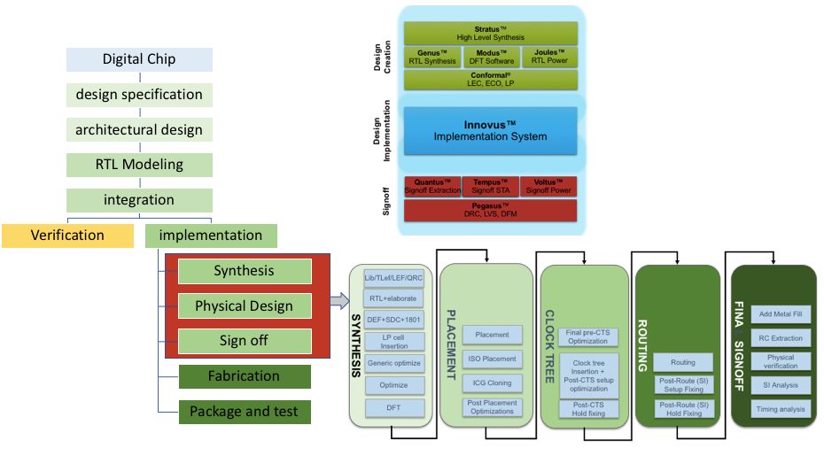
The entire implementation phase can be summarized as playing with EDA tools and methodologies based on EDA tools. EDA tools are undoubtedly dominant in the implementation phase. The quality of a chip largely depends on the engineer’s skills before the implementation phase, and after the implementation phase, it mainly depends on how well the EDA tools are utilized. The entire design implementation process involves many tools. Here are four main players; the blank parts do not mean there are none, just that I am unaware.
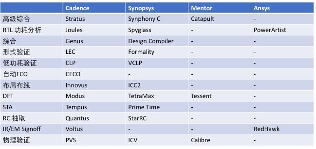
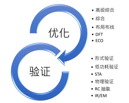
The digital circuit implementation process can be broadly divided into two parts: optimization and verification. Optimization may change the logical description method, alter the logical structure, and insert new logic, all of which carry the risk of introducing errors, so verification tools are needed for monitoring; verification ensures that the logic optimization process does not change logical functionality, meets timing requirements, has no physical rule violations, and ensures signal integrity. All these verifications have a corresponding set of passing rules, and if any one of them does not meet the standard, it cannot be sent for production.
High-level synthesis: High-level synthesis refers to converting design intentions described in C/C++/System C into RTL described in Verilog/System Verilog, mainly used in computation logic-dominated designs. Besides the three giants, many small companies also perform well in this area.
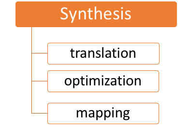
Synthesis: In the implementation process, in terms of the underlying algorithms, synthesis is undoubtedly the most difficult and complex part. Synthesis first converts the logic described in Verilog/System Verilog/VHDL into logic described by Gtech, then optimizes the Gtech logic and finally maps the optimized Gtech description to the corresponding technology library. The optimization process involves multiple aspects. In recent years, the development direction of EDA tools can be summarized as: capacity, speed, and correlation. Capacity: refers to the design scale that can be handled; speed: refers to the optimization speed of EDA tools; correlation: refers to the correlation with layout and routing. Mainstream tools: Genus, Design Compiler. In this regard, it is almost impossible for any latecomer to emerge, unless one day the entire methodology of digital circuit design undergoes a revolutionary change.
DFT: Insert compression and decompression logic, insert scan chains, insert Mbist, insert Lbist, insert Boundary Scan, insert OCC, insert Test Points, generate ATPG patterns, and perform fault diagnosis. DFT engineers are like traditional Chinese medicine practitioners who insert, observe, and diagnose. Currently, there is a shortage of DFT engineers in the market, making them expensive! Mainstream tools: Tessenst, Modus, TetraMax.
ECO: Whenever something new is introduced, it may introduce bugs. Early detection of bugs allows for a re-run of the implementation process, but if bugs are found later, redoing the process would be too costly. The usual practice is to use ECO. For simple bug fixes, manual ECO can suffice, but for complex bug fixes, manual ECO may be inadequate, so EDA tools are needed to complete the corresponding tasks. Currently, the best automatic ECO tool on the market is Conformal ECO. Recently, some startups have been making corresponding point tools, but without their own synthesis tools to optimize the ECO patches, it is challenging to achieve good results.
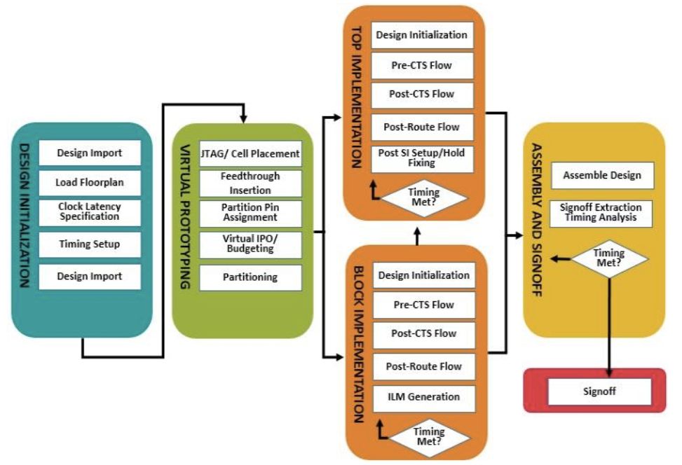
Layout and Routing: Before entering the nanometer era, layout and routing were not that complex. Since 90nm to the present 3nm, the complexity of layout and routing has grown exponentially. From floorplan to placement to CTS to routing, each step involves algorithms that have undergone revolutionary changes in recent years, starting with the emergence of Innovus, marking a new era in layout and routing. Amid the wave of AI, C and S have both dived in, aiming to create the smartest layout and routing tools in the world. Perhaps one day, it will be as easy as conversing with a smart assistant:
-
Silicon Farmer: Innovus, please analyze file A and generate the most power-efficient result based on the set goals;
-
Innovus: The target file has been read. Based on the design data analysis, this design will require approximately 250G of memory and will be completed within 5 hours. Please choose whether to automatically proceed to the next task after completion…
RTL Power Analysis: This step can be done during implementation or before implementation. The analysis process is relatively simple: read in RTL, SDC, simulation stimuli, and analyze average and instantaneous power consumption to identify “power defects” in the design, guiding designers for optimization. Mainstream tools include: Joules, Spyglass, PowerArtist.
Formal Verification: Throughout the implementation process, formal verification acts as the inspector of logical functional equivalence. After any optimization step, formal verification is required to ensure that logical functionality has not been altered during the optimization process. Mainstream tools: LEC, Formality. With the explosive growth of design scale and the rapid development of optimization techniques, the difficulty of formal verification has gradually increased, consuming more time, with SmartLEC being a pioneer for complex designs.
Low Power Verification: For low-power designs, low-power verification must validate the syntax semantics and descriptive intentions of CPF/UPF/1801, ensuring that low-power units are not over-inserted, under-inserted, or mis-inserted, that power and ground connections meet design intentions, and that electrical characteristics are intact. Mainstream tools: CLP.
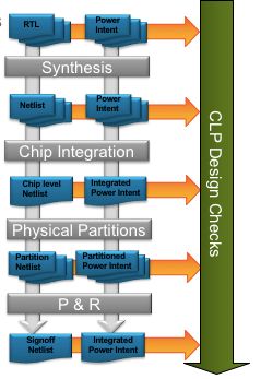
STA: Timing signoff, STA seems complex, but it is not. Compared to the optimization process, it is much simpler. Setting aside Timing ECO, all actions in STA are merely calculations, not problem-solving. An inappropriate analogy: STA is like a kindergarten arithmetic problem where the addends are already there, and you only need to find the sum; whereas the optimization process seeks the optimal or near-optimal solution, which is much more challenging. In recent years, STA EDA tools have focused on several directions: how to simulate random process variations during manufacturing, how to handle large-scale designs, and how to simulate the impact of new technology node electrical characteristics on timing.
Power Signoff: Validate whether the design’s power network is robust enough, analyze, discover, and correct: IR-drop and EM. Mainstream tools: Voltus, RedHawk.
Physical Verification: Verify whether all transistors, vias, and routing meet the rules set by the foundry. This is a labor-intensive task, similar to cleaning up the garbage after building a house. Mainstream tools: Calibre, PVS, ICV.
The entire digital implementation process involves many tools, with the three giants leading the way, and there are hardly any followers. Occasionally, some latecomers excel in specific point tools, but most will be acquired by the three giants. This is also an industry pattern. In terms of market value, the three giants combined are not as hefty as a leg of an internet company; however, they are indispensable in the entire chip design implementation process. For our country to strengthen its chip industry, we must increase investment in EDA to move further away from being choked by the throat.
Transferred from: “Industry Intelligent Official”