In embedded vision systems, FPGAs have become the preferred solution for video signal processing due to their parallel processing advantages. HDMI, as a mainstream high-definition video interface, serves as the foundational scenario for signal conversion in FPGA visual applications. This article provides a practical FPGA RGB to HDMI display solution based on the XC7Z015CLG485-2I development board, covering core principles, module design, and complete implementation code.
01
—
FPGA RGB to HDMI Principles
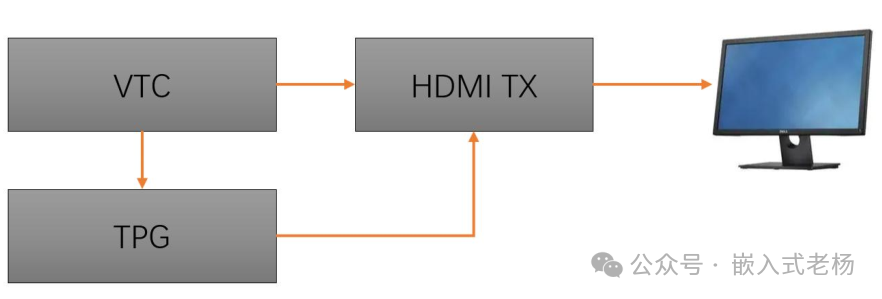
HDMI (High-Definition Multimedia Interface) transmits video data using TMDS (Transition-Minimized Differential Signaling) encoding technology. The core of this process is to integrate 8-bit RGB pixel data, horizontal and vertical sync signals (HS/VS), and data enable signals (DE) into 10-bit differential signals, achieving high-speed serial transmission with a 5x pixel clock. The core process for converting RGB to HDMI using FPGA involves: generating a 1x pixel clock (PCLKX1) and a 5x pixel clock (PCLKX5) through clock management IP; the Video Timing Controller (VTC) produces HS/VS/DE signals that meet resolution requirements; the Test Pattern Generator (TPG) generates RGB test data; and the HDMI TX module completes TMDS encoding and serial differential output, ultimately driving the display through the HDMI interface.
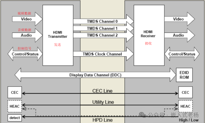
The interactive principle of HDMI data transmission:
After the HDMI sender receives video, audio, and control signals, it encodes and transmits these signals to the HDMI receiver through three TMDS data channels and one TMDS clock channel. The EDID ROM on the receiver side will feedback the display’s supported parameters (such as resolution) to the sender via the Display Data Channel (DDC). Meanwhile, the CEC line facilitates control interaction between devices, the HEAC line handles auxiliary function transmission, and the HPD line detects and reports hot-plug status, thus achieving complete bidirectional interaction and transmission of audio, video, and control signals.
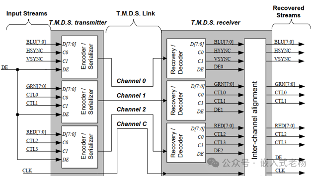
The transmission principle of TMDS in HDMI:
The left TMDS transmitter receives blue/green/red pixel data, sync signals, control signals, and clock inputs. Each channel (including data channels 0-2 and clock channel C) first encodes the parallel signals and then converts them into serial signals for transmission over the TMDS link. The right TMDS receiver recovers and decodes the serial signals from each channel back into parallel format, aligns the channels, and ultimately restores the signal stream to match the input, achieving high-speed and reliable transmission of audio, video, and control signals..
02
—
Case Function Introduction
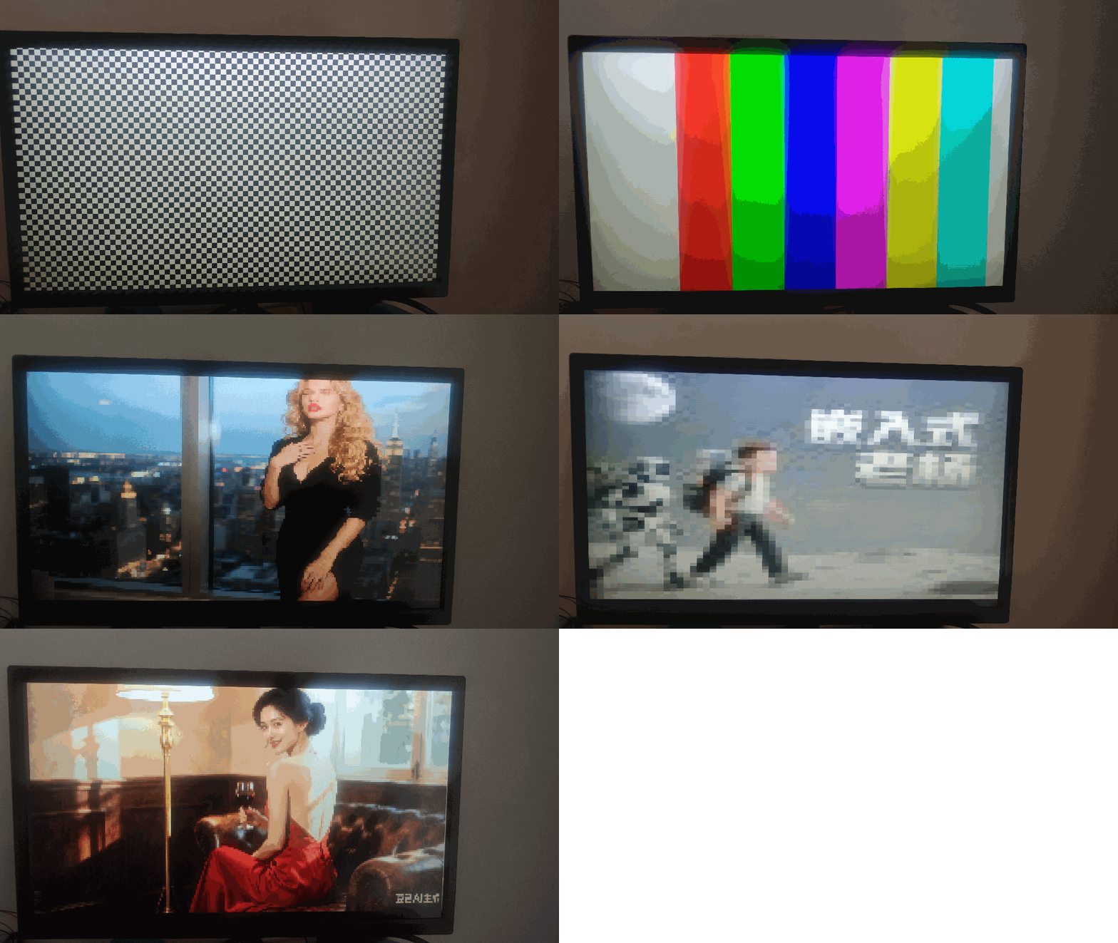
This case is based on the XC7Z015CLG485-2I FPGA, with an external 100MHz crystal oscillator input, achieving HDMI display functionality at a resolution of 720P (1280×720). The system integrates four core modules: clock management, video timing control, test pattern generation, and HDMI encoding output. The TPG supports three test modes: grid, color bars, and images (limited by RAM resources for demonstration, using a resolution of 256×144), which cycle through. The HDMI output complies with TMDS standards and can be directly connected to a standard HDMI display to show stable images.
1. VTC Video Timing Controller (uivtc)
Based on line and field counters, it generates video timing signals that comply with HDMI standards by configuring parameters such as the number of valid pixels per line and field, and sync start/end positions to adapt to different resolutions (this case is for 720P). The core logic involves: the horizontal counter (hcnt) traverses all clock cycles of a line, while the vertical counter (vcnt) accumulates at the end of a line, generating HS (horizontal sync), VS (vertical sync), and DE (data enable) signals based on the counter values, while ensuring timing stability through sync reset.
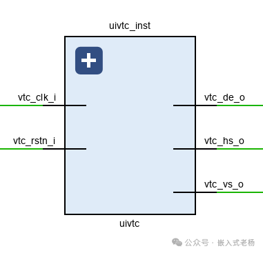
Module Interface:
-
Input: vtc_clk_i (timing clock, i.e., PCLKX1), vtc_rstn_i (asynchronous reset, active high)
-
Output: vtc_hs_o (horizontal sync signal), vtc_vs_o (vertical sync signal), vtc_de_o (data enable signal)
2. TPG Video Test Pattern Generator (uitpg)
During the DE signal active period, it generates specified test patterns based on the line and field counters (h_cnt/v_cnt), supporting mode cycling. The grid mode generates a black and white grid through high-bit XOR of the counters; the color bar mode outputs different RGB colors segmented by horizontal pixels; the image mode reads pre-stored image data from ROM and outputs it after address scaling.
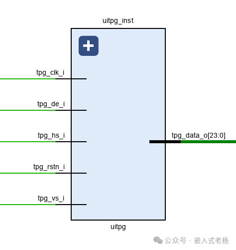
Module Interface:
-
Input: tpg_clk_i (working clock, i.e., PCLKX1), tpg_rstn_i (asynchronous reset, active high), tpg_hs_i/vs_i/de_i (timing signals output from VTC)
-
Output: tpg_data_o (24-bit RGB pixel data), tpg_hs_o/vs_o/de_o (timing signals direct output)
3. HDMI TX Encoding Module (uihdmitx)
Divided into TMDS encoding and 10:1 serialization. The TMDS encoder encodes 8-bit RGB data and sync signals into 10-bit minimum transition differential signals. Depending on the FPGA series (7FAMILY/ULTRASCALE), the corresponding serializer (oserdese2/oserdese3) is selected to convert 10-bit parallel data into serial differential signals under the drive of a 5x pixel clock, outputting HDMI clock and data differential pairs.
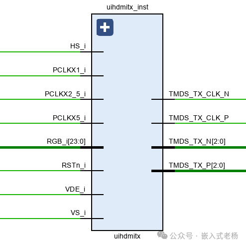
Module Interface:
-
Input: RSTn_i (reset, active low), HS_i/VS_i/VDE_i (timing signals), RGB_i (24-bit RGB data), PCLKX1_i (1x pixel clock), PCLKX5_i (5x pixel clock)
-
Output: TMDS_TX_CLK_P/N (HDMI clock differential pair), TMDS_TX_P/N [2:0] (HDMI data differential pairs)
03
—
Hardware Principles
The RCtamp0524 chip (U17) provides ESD protection for HDMI differential data, clock, and control signals. The HDMI_HP end utilizes IN5822 and D3 to handle the power path for hot-plug detection. The differential signal path is configured with 49.9Ω termination resistors (R70/R71) for impedance matching, along with 0.1μF decoupling capacitors (C81-C88) to stabilize the power supply. The SDA/SCL signals of the DDC channel achieve 3.3V to 5V level conversion through AO3400 transistors (Q1/Q2) combined with pull-up resistors, while all differential signals follow the “all equal length, internal equal length” wiring rule to ensure high-speed timing consistency, ultimately achieving stable transmission of HDMI signals and reliable interface protection.
04
—
Code Implementation
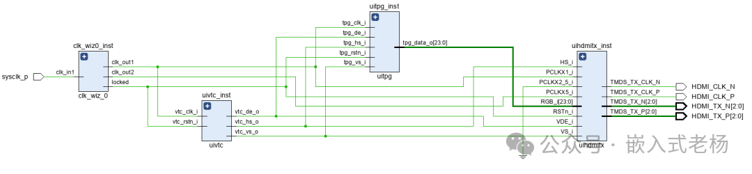
1. Top-Level Module (display.v)
module display(input sysclk_p, // System clock inputoutput HDMI_CLK_P, // HDMI output clock P output HDMI_CLK_N, // HDMI output clock N output [2:0]HDMI_TX_P, // HDMI output data P output [2:0]HDMI_TX_N // HDMI output data N); // Define internal interconnection signals (timing, clock, RGB data) wire vtc_vs,vtc_hs,vtc_de; wire pclkx1,pclkx5,locked; wire [7:0] rgb_r,rgb_g,rgb_b; // Bind internal pixel clock to PCLKX1 (1x clock) assign vtc_clk = pclkx1; // Use PLL locked signal as system asynchronous reset (active high) assign vtc_rstn = locked; // Instantiate PLL/MMCM clock management IP to generate 1x/5x pixel clocks and locked signal clk_wiz_0 clk_wiz0_inst(.clk_out1(pclkx1),.clk_out2(pclkx5),.locked(locked),.clk_in1(sysclk_p)); // Instantiate HDMI output IP to encode RGB data and timing signals into HDMI differential signals uihdmitx #(.FAMILY("7FAMILY")) uihdmitx_inst(.RSTn_i(locked),.HS_i(vtc_hs),.VS_i(vtc_vs),.VDE_i(vtc_de),.RGB_i({rgb_r,rgb_g,rgb_b}),.PCLKX1_i(pclkx1),.PCLKX2_5_i(1'b0),.PCLKX5_i(pclkx5),.TMDS_TX_CLK_P(HDMI_CLK_P),.TMDS_TX_CLK_N(HDMI_CLK_N),.TMDS_TX_P(HDMI_TX_P),.TMDS_TX_N(HDMI_TX_N)); // Instantiate VTC module to generate 720P resolution video timing signals (HS/VS/DE) uivtc#(.H_ActiveSize(1280),.H_FrameSize(1280+88+44+239),.H_SyncStart(1280+88),.H_SyncEnd(1280+88+44),.V_ActiveSize(720),.V_FrameSize(720+4+5+28),.V_SyncStart(720+4),.V_SyncEnd(720+4+5)) uivtc_inst(.vtc_clk_i(vtc_clk),.vtc_rstn_i(vtc_rstn),.vtc_vs_o(vtc_vs),.vtc_hs_o(vtc_hs),.vtc_de_o(vtc_de)); // Instantiate TPG module to generate test image RGB data based on VTC timing uitpg uitpg_inst (.tpg_clk_i(vtc_clk),.tpg_rstn_i(vtc_rstn),.tpg_vs_i(vtc_vs),.tpg_hs_i(vtc_hs),.tpg_de_i(vtc_de),.tpg_vs_o(),.tpg_hs_o(),.tpg_de_o(),.tpg_data_o({rgb_r,rgb_g,rgb_b})); endmodule2. VTC Module (vtc.v)
module uivtc#(parameter H_ActiveSize = 1980,parameter H_FrameSize = 1920+88+44+148,parameter H_SyncStart = 1920+88,parameter H_SyncEnd = 1920+88+44,parameter V_ActiveSize = 1080,parameter V_FrameSize = 1080+4+5+36,parameter V_SyncStart = 1080+4,parameter V_SyncEnd = 1080+4+5)(input vtc_rstn_i,input vtc_clk_i,output reg vtc_vs_o,output reg vtc_hs_o,output reg vtc_de_o); // Define horizontal counter, vertical counter, reset counter, and sync reset signal reg [11:0] hcnt = 12'd0; reg [11:0] vcnt = 12'd0; reg [2:0] rst_cnt = 3'd0; wire rst_sync = rst_cnt[2]; // Generate sync reset signal (to avoid asynchronous reset metastability) always @(posedge vtc_clk_i or negedge vtc_rstn_i) begin if(vtc_rstn_i == 1'b0) rst_cnt <= 3'd0; else if(rst_cnt[2] == 1'b0) rst_cnt <= rst_cnt + 1'b1; end // Horizontal counter: traverses all clock cycles of a line (0~H_FrameSize-1) always @(posedge vtc_clk_i) begin if(rst_sync == 1'b0) hcnt <= 12'd0; else if(hcnt < (H_FrameSize - 1'b1)) hcnt <= hcnt + 1'b1; else hcnt <= 12'd0; end // Vertical counter: accumulates after a line ends, traverses all lines of a frame (0~V_FrameSize-1) always @(posedge vtc_clk_i) begin if(rst_sync == 1'b0) vcnt <= 12'd0; else if(hcnt == (H_ActiveSize - 1'b1)) begin vcnt <= (vcnt == (V_FrameSize - 1'b1)) ? 12'd0 : vcnt + 1'b1; end end // Combinational logic generates HS/VS/DE raw signals wire hs_valid = hcnt < H_ActiveSize; wire vs_valid = vcnt < V_ActiveSize; wire vtc_hs = (hcnt >= H_SyncStart && hcnt < H_SyncEnd); wire vtc_vs = (vcnt > V_SyncStart && vcnt <= V_SyncEnd); wire vtc_de = hs_valid && vs_valid; // Timing signals are clocked out to improve timing performance (eliminate combinational logic delay) always @(posedge vtc_clk_i) begin if(rst_sync == 1'b0) begin vtc_vs_o <= 1'b0; vtc_hs_o <= 1'b0; vtc_de_o <= 1'b0; end else begin vtc_vs_o <= vtc_vs; vtc_hs_o <= vtc_hs; vtc_de_o <= vtc_de; end end endmodule
3. TPG Module (tpg.v)
module uitpg(input tpg_clk_i,input tpg_rstn_i,input tpg_vs_i,input tpg_hs_i,input tpg_de_i,output tpg_vs_o,output tpg_hs_o,output tpg_de_o,output [23:0] tpg_data_o); // Define internal registers, pattern data registers, display mode, and ROM interface signals reg tpg_vs_r = 1'b0; reg tpg_hs_r = 1'b0; reg [7:0] grid_data = 8'd0; reg [23:0] color_bar = 24'd0; reg [10:0] dis_mode = 11'd0; reg [7:0] r_reg = 8'd0; reg [7:0] g_reg = 8'd0; reg [7:0] b_reg = 8'd0; wire [15:0] pic_addr; wire [23:0] pic_data_1, pic_data_2, pic_data_3, pic_data_4; reg [23:0] pic_data_reg = 24'd0; // Store input timing signals, synchronize data generation rhythm always @(posedge tpg_clk_i) begin tpg_vs_r <= tpg_vs_i; tpg_hs_r <= tpg_hs_i; end // Define row/column counters for pattern coordinate positioning reg [11:0] v_cnt = 12'd0; reg [11:0] h_cnt = 12'd0; // Column counter: accumulates when DE is active, resets when inactive always @(posedge tpg_clk_i) h_cnt <= tpg_de_i ? h_cnt + 1'b1 : 12'd0; // Row counter: resets when VS is active, accumulates on HS rising edge always @(posedge tpg_clk_i) if(tpg_vs_i) v_cnt <= 12'd0; else v_cnt <= ((!tpg_hs_r) && tpg_hs_i) ? v_cnt + 1'b1 : v_cnt; // Display mode switching: switches once per frame, cycles 0~4 always @(posedge tpg_clk_i) if((tpg_rstn_i==1'b0) || dis_mode[10:7] > 4'd4) dis_mode <= 0; else dis_mode <= ((!tpg_vs_r) && tpg_vs_i) ? dis_mode + 1'b1 : dis_mode; // Generate black and white grid pattern (5x5 grid, high-bit XOR of counters) always @(posedge tpg_clk_i) begin grid_data <= ((v_cnt[4]==1'b1) ^ (h_cnt[4]==1'b1)) ? 8'h00 : 8'hff; end // Generate RGB color bar pattern (8 segments, segmented by column counter) always @(posedge tpg_clk_i) begin if(h_cnt==260) color_bar <= 24'hff0000; else if(h_cnt==420) color_bar <= 24'h00ff00; else if(h_cnt==580) color_bar <= 24'h0000ff; else if(h_cnt==740) color_bar <= 24'hff00ff; else if(h_cnt==900) color_bar <= 24'hffff00; else if(h_cnt==1060) color_bar <= 24'h00ffff; else if(h_cnt==1220) color_bar <= 24'hffffff; else if(h_cnt==1380) color_bar <= 24'h000000; else color_bar <= color_bar; end // Calculate image ROM read address (coordinate scaling by 5, adapting to 256x144 image) assign pic_addr = ((v_cnt / 5) * 256) + (h_cnt / 5); // Instantiate 3 image ROMs to store different test image data blk_mem_gen_0 picture_rom_inst1 (.clka(tpg_clk_i),.addra(pic_addr[15:0]),.douta(pic_data_1)); blk_mem_gen_1 picture_rom_inst2 (.clka(tpg_clk_i),.addra(pic_addr[15:0]),.douta(pic_data_2)); blk_mem_gen_2 picture_rom_inst3 (.clka(tpg_clk_i),.addra(pic_addr[15:0]),.douta(pic_data_3)); // ROM address boundary check to avoid out-of-bounds access reg [15:0] safe_pic_addr; always @(posedge tpg_clk_i) begin if (pic_addr < 36864) safe_pic_addr <= pic_addr; else safe_pic_addr <= 16'd0; end // Generate debug coordinate signals (scaled row/column coordinates) reg [11:0] debug_v = 0; reg [11:0] debug_h = 0; always @(posedge tpg_clk_i) begin debug_v <= v_cnt / 5; debug_h <= h_cnt / 5; end // Select output RGB data based on display mode (grid/color bar/image) always @(posedge tpg_clk_i) begin case(dis_mode[10:7]) 4'd0:begin r_reg <= grid_data; g_reg <= grid_data; b_reg <= grid_data; end 4'd1:begin r_reg <= color_bar[23:16]; g_reg <= color_bar[15:8]; b_reg <= color_bar[7:0]; end 4'd2:begin r_reg <= pic_data_1[23:16]; g_reg <= pic_data_1[15:8]; b_reg <= pic_data_1[7:0]; end 4'd3:begin r_reg <= pic_data_2[23:16]; g_reg <= pic_data_2[15:8]; b_reg <= pic_data_2[7:0]; end 4'd4:begin r_reg <= pic_data_3[23:16]; g_reg <= pic_data_3[15:8]; b_reg <= pic_data_3[7:0]; end default:begin r_reg <= 0; g_reg <= 0; b_reg <= 0; end endcase end // Bind output signals (RGB data and timing direct output signals) assign tpg_data_o = {r_reg,g_reg,b_reg}; assign tpg_vs_o = tpg_vs_i; assign tpg_hs_o = tpg_hs_i; assign tpg_de_o = tpg_de_i; endmodule
4. HDMI TX Module (hdmi_tx.v)
module uihdmitx#(parameter FAMILY = "ULTRASCALE")(input RSTn_i,input VS_i,input HS_i,input VDE_i,input [23:0] RGB_i,input PCLKX1_i,input PCLKX2_5_i,input PCLKX5_i,output TMDS_TX_CLK_P,output TMDS_TX_CLK_N,output [2:0]TMDS_TX_P,output [2:0]TMDS_TX_N); // Split 24-bit RGB data into R/G/B single-channel 8-bit data wire [7:0] RED = RGB_i[23:16]; wire [7:0] GREEN = RGB_i[15:8]; wire [7:0] BLUE = RGB_i[7:0]; // Define 10-bit parallel data signals after TMDS encoding wire [9:0] intTmdsRed; wire [9:0] intTmdsGreen; wire [9:0] intTmdsBlue; // Convert active low reset to active high wire intRst = !RSTn_i; // Instantiate R channel TMDS encoder, encoding 8-bit R data to 10-bit TMDS code TMDSEncoder Inst_TMDSEncoder_red(.D_I(RED),.C0_I(1'b0),.C1_I(1'b0),.DE_I(VDE_i),.CLK_I(PCLKX1_i),.D_O(intTmdsRed)); // Instantiate G channel TMDS encoder, encoding 8-bit G data to 10-bit TMDS code TMDSEncoder Inst_TMDSEncoder_green(.D_I(GREEN),.C0_I(1'b0),.C1_I(1'b0),.DE_I(VDE_i),.CLK_I(PCLKX1_i),.D_O(intTmdsGreen)); // Instantiate B channel TMDS encoder, encoding 8-bit B data + sync signals to 10-bit TMDS code TMDSEncoder Inst_TMDSEncoder_blue(.D_I(BLUE),.C0_I(HS_i),.C1_I(VS_i),.DE_I(VDE_i),.CLK_I(PCLKX1_i),.D_O(intTmdsBlue)); // Select corresponding 10:1 serializer based on FPGA series (ULTRASCALE/7FAMILY) generate if(FAMILY == "ULTRASCALE" || FAMILY == "ULTRASCALE_PLUS") begin : ULTRASCALE_FAMILY // Instantiate ULTRASCALE series HDMI clock serializer, generating TMDS clock differential signals oserdese3_10to1 #(.FAMILY(FAMILY)) Inst_clk_oserdese3_10to1(.txdata("1111100000"),.txrst(intRst),.pclk(PCLKX1_i),.clkdiv2(PCLKX5_i),.clkdiv4(PCLKX2_5_i),.tx_p(TMDS_TX_CLK_P),.tx_n(TMDS_TX_CLK_N)); // Instantiate R channel data serializer, converting 10-bit TMDS parallel data to serial differential signals oserdese3_10to1#(.FAMILY(FAMILY)) Inst_d2_serializer_10_1(.txdata(intTmdsRed),.txrst(intRst),.pclk(PCLKX1_i),.clkdiv2(PCLKX5_i),.clkdiv4(PCLKX2_5_i),.tx_p(TMDS_TX_P[2]),.tx_n(TMDS_TX_N[2])); // Instantiate G channel data serializer, converting 10-bit TMDS parallel data to serial differential signals oserdese3_10to1#(.FAMILY(FAMILY)) Inst_d1_serializer_10_1(.txdata(intTmdsGreen),.txrst(intRst),.pclk(PCLKX1_i),.clkdiv2(PCLKX5_i),.clkdiv4(PCLKX2_5_i),.tx_p(TMDS_TX_P[1]),.tx_n(TMDS_TX_N[1])); // Instantiate B channel data serializer, converting 10-bit TMDS parallel data to serial differential signals oserdese3_10to1#(.FAMILY(FAMILY)) Inst_d0_serializer_10_1(.txdata(intTmdsBlue),.txrst(intRst),.pclk(PCLKX1_i),.clkdiv2(PCLKX5_i),.clkdiv4(PCLKX2_5_i),.tx_p(TMDS_TX_P[0]),.tx_n(TMDS_TX_N[0])); end else if(FAMILY == "7FAMILY") begin : family_7 // Instantiate 7FAMILY series HDMI clock serializer, generating TMDS clock differential signals oserdese2_10to1 Inst_clk_oserdese2_10to1(.txdata("1111100000"),.txrst(intRst),.pclk(PCLKX1_i),.clkdiv2(PCLKX5_i),.tx_p(TMDS_TX_CLK_P),.tx_n(TMDS_TX_CLK_N)); // Instantiate R channel data serializer, converting 10-bit TMDS parallel data to serial differential signals oserdese2_10to1 Inst_d2_serializer_10_1(.txdata(intTmdsRed),.txrst(intRst),.pclk(PCLKX1_i),.clkdiv2(PCLKX5_i),.tx_p(TMDS_TX_P[2]),.tx_n(TMDS_TX_N[2])); // Instantiate G channel data serializer, converting 10-bit TMDS parallel data to serial differential signals oserdese2_10to1 Inst_d1_serializer_10_1(.txdata(intTmdsGreen),.txrst(intRst),.pclk(PCLKX1_i),.clkdiv2(PCLKX5_i),.tx_p(TMDS_TX_P[1]),.tx_n(TMDS_TX_N[1])); // Instantiate B channel data serializer, converting 10-bit TMDS parallel data to serial differential signals oserdese2_10to1 Inst_d0_serializer_10_1(.txdata(intTmdsBlue),.txrst(intRst),.pclk(PCLKX1_i),.clkdiv2(PCLKX5_i),.tx_p(TMDS_TX_P[0]),.tx_n(TMDS_TX_N[0])); end endgenerate endmodule
5. Timing Constraint File (fpga_io.xdc)
# Set system clock period to 10ns (100MHz) create_clock -period 10.000 -name sysclk [get_ports sysclk_p] # Bind system clock input pin to L5 set_property PACKAGE_PIN L5 [get_ports sysclk_p] # Set system clock pin IO standard to LVCMOS33 set_property IOSTANDARD LVCMOS33 [get_ports sysclk_p] # Bind HDMI clock P pin to T2 set_property PACKAGE_PIN T2 [get_ports HDMI_CLK_P] # Bind HDMI R channel P pin to U2 set_property PACKAGE_PIN U2 [get_ports HDMI_TX_P[2]] # Bind HDMI G channel P pin to M2 set_property PACKAGE_PIN M2 [get_ports HDMI_TX_P[1]] # Bind HDMI B channel P pin to L6 set_property PACKAGE_PIN L6 [get_ports HDMI_TX_P[0]] # Set HDMI clock pin IO standard to TMDS_33 set_property IOSTANDARD TMDS_33 [get_ports HDMI_CLK_P] # Set HDMI data pin IO standard to TMDS_33 set_property IOSTANDARD TMDS_33 [get_ports HDMI_TX_P[*]] # Enable BIT file compression to reduce storage usage set_property BITSTREAM.GENERAL.COMPRESS true [current_design]
6. Python Script to Convert Image to .COE File (png_to_coe.py)
from PIL import Image import numpy as np import os def png_to_coe_256x144(png_path, coe_path): try: # Open the image and check basic information img = Image.open(png_path) print(f"Original image format: {img.format}, mode: {img.mode}, size: {img.size}") # Convert to RGB mode if img.mode != 'RGB': img = img.convert('RGB') print("Converted to RGB mode") # Resize img = img.resize((256, 144)) print(f"Resized dimensions: {img.size}") # Convert to numpy array img_array = np.array(img) print(f"Image array shape: {img_array.shape}") print(f"Data type: {img_array.dtype}") # Check the values of the first few pixels print("First 5 pixels RGB values:") for i in range(min(5, 144)): for j in range(min(5, 256)): r, g, b = img_array[i, j] print(f"Pixel[{i},{j}]: R={r:3d}, G={g:3d}, B={b:3d}") with open(coe_path, 'w') as f: f.write("memory_initialization_radix=16;\n") f.write("memory_initialization_vector=\n") pixel_count = 0 for i in range(144): for j in range(256): r, g, b = img_array[i, j] # Ensure values are in the range 0-255 r = max(0, min(255, r)) g = max(0, min(255, g)) b = max(0, min(255, b)) # 24-bit RGB format: R[23:16], G[15:8], B[7:0] rgb_24bit = (int(r) << 16) | (int(g) << 8) | int(b) # Debug: Check the conversion of the first few pixels if pixel_count < 5: print(f"Before conversion: R={r:3d}, G={g:3d}, B={b:3d}") print(f"After conversion: 0x{rgb_24bit:06X}") # Write to COE file f.write(f"{rgb_24bit:06X}") pixel_count += 1 # Check if it's the last data if i == 143 and j == 255: f.write(";\n") else: f.write(",\n") print(f"Total processed {pixel_count} pixels") print(f"COE file generated successfully: {coe_path}") return True except Exception as e: print(f"Error: {e}") import traceback traceback.print_exc() return False # Create a test image to verify def create_test_image(): """Create a test image with red, green, blue, and white areas""" from PIL import Image import numpy as np # Create a 256x144 test image img_array = np.zeros((144, 256, 3), dtype=np.uint8) # Top left: red (255,0,0) img_array[0:72, 0:128] = [255, 0, 0] # Top right: green (0,255,0) img_array[0:72, 128:256] = [0, 255, 0] # Bottom left: blue (0,0,255) img_array[72:144, 0:128] = [0, 0, 255] # Bottom right: white (255,255,255) img_array[72:144, 128:256] = [255, 255, 255] # Add some gradient areas for i in range(72, 144): for j in range(128, 256): img_array[i, j] = [j - 128, i - 72, 128] # Gradient effect test_img = Image.fromarray(img_array) test_img.save("test_image.png") print("Test image generated: test_image.png") return "test_image.png" # Use if __name__ == "__main__": # Method 1: Use test image print("=== Method 1: Use test image ===") test_image_path = create_test_image() success = png_to_coe_256x144(test_image_path, "test_image.coe") if success: # Check the first few lines of the generated COE file print("\nCheck the first few lines of the COE file:") with open("test_image.coe", 'r') as f: for i, line in enumerate(f): if i < 10: # Only show the first 10 lines print(f"Line {i + 1}: {line.strip()}") else: break # Method 2: Use your original image print("\n=== Method 2: Use your image ===") original_image = "C:/Users/Administrator/Desktop/fpga_demo/CH25_rgb2hdmi_test/4.png" if os.path.exists(original_image): png_to_coe_256x144(original_image, "C:/Users/Administrator/Desktop/fpga_demo/CH25_rgb2hdmi_test/image_data4_256x144.coe") else: print(f"Original image does not exist: {original_image}")05
—
Run Results
Environment Configuration: Vivado 2021.1, XC7Z015CLG485-2I development board, 100MHz external crystal oscillator, HDMI display; Python script using Pycharm 2022.2.3.
Project Build: Create a Verilog project, add all the above module files, generate clk_wiz_0 IP (input 100MHz, output 74.25MHz and 371.25MHz), generate 3 blk_mem_gen IPs and load 256×144 24-bit RGB image data.
Download and Run: Synthesize, implement, generate bitstream file, and download to FPGA. Connect the HDMI display to the development board HDMI interface to observe:
-
The display recognizes 720P resolution with no signal loss;
-
The screen cycles through a grid (black and white 5×5 grid), color bars (red/green/blue/purple/yellow/cyan/white/black 8 segments), and pre-stored images, with a switching period of about 1 second/frame.
Previous Articles:
FPGA I2C Communication Example
FPGA SPI Communication Example
FPGA Serial Communication Example
Low Power Design Methods in Verilog
Common Hardware Implementations and Principles in Verilog
Sync FIFO and Async FIFO
Verilog Clock Division
Verilog Reset Design
FPGA Cross-Clock Domain Design
Usage of Functions and Tasks in Verilog Development