According to sources cited by Wccftech, the Japanese semiconductor company Rapidus is preparing its advanced 2nm process node, named “2HP,” which is expected to achieve logic density comparable to TSMC’s N2 and significantly surpass Intel’s 18A.
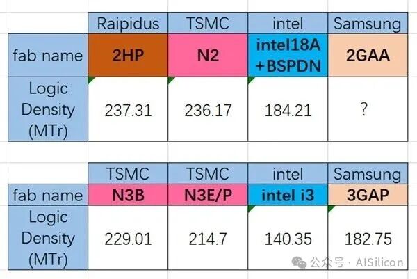
Reportedly, the logic density of Rapidus’s 2HP node will reach 237.31 MTr/mm², which is nearly on par with TSMC’s N2 at 236.17 MTr/mm². The report further indicates that both nodes utilize a high-density (HD) cell library — based on a G45 pitch and a height of 138 unit cells, designed to maximize logic density, suggesting that their transistor counts are similar.
As for Intel, despite its 18A node having a smaller process size, the reported logic density is 184.21 MTr/mm² — a relatively low density. The report cites sources explaining that Intel’s use of backside power delivery network (BSPDN) is the reason for this outcome, as it occupies part of the front metal layer space, reducing the density measured in the high-density (HD) cell library. However, the report also notes that Intel is more focused on performance per watt rather than pure density, indicating that higher logic density is not its primary goal, especially since the 18A node is mainly for internal use.
Rapidus’s 2nm PDK (Process Design Kit) is scheduled for release in the first quarter of 2026, with a target for mass production in 2027. This Japanese company is rapidly advancing. According to TechPowerUp, Rapidus has successfully completed the tape-out of a 2nm GAA (Gate-All-Around) test chip, aiming for mass production in 2027. The report adds that the chip is manufactured using ASML’s extreme ultraviolet (EUV) lithography tools and has met all initial electrical performance metrics. Looking ahead to mass production in 2027, Rapidus’s CEO stated that its IIM-1 factory in Hokkaido is expected to produce approximately 25,000 wafers per month.
TechPowerUp also noted that by 2027, Rapidus’s process level may lag behind TSMC by one to two nodes, and possibly even behind Intel. The report adds that to differentiate itself in competition, the company is focusing on production flexibility and emphasizes its unique full-wafer processing technology that can shorten the production cycle to just 50 days, while traditional batch and single-wafer mixed processes typically require about 120 days.
Follow for more updates⭐