Challenges and Future Evolution of Optical Module Technology on PCBs
As the core interconnection unit of computing infrastructure such as data centers and 5G communications, optical modules have undergone a technological evolution from 100G to 400G, 800G, and even 1.6T, which has imposed comprehensive technical reconstruction requirements on the PCBs (Printed Circuit Boards) that carry their circuits and optoelectronic components. PCBs have transitioned from traditional electronic signal carriers to key components that determine the performance limits, manufacturability, and long-term reliability of optical modules, forming a deep binding with the development of optical modules.
1. Core Challenges Faced by PCBs Under Optical Module Technology Upgrades
The pressure from the exponential growth in signal rates and breakthroughs in integration is continuously impacting the material selection, process precision, and design logic of PCBs. The specific challenges are concentrated in the following four areas:
(1) Integrity Dilemma of High-Speed Signal Transmission
The exponential increase in signal rates (from 25Gbps to 112Gbps and above) has dramatically amplified the signal transmission loss issues in PCBs. According to signal integrity theory, signal loss is proportional to the square root of frequency, and the high-frequency harmonic components of 112Gbps PAM4 signals significantly compound conductor and dielectric losses.
- Loss Control Challenges: Traditional FR4 substrates (dielectric constant Dk=4.4, loss factor Df=0.010~0.015) can no longer meet the requirements, as their dielectric losses can lead to severe signal attenuation until the eye diagram closes. Additionally, the skin effect losses caused by the roughness of copper foil surfaces become a major source of conductor loss at high frequencies.
- Impedance Matching Conflicts: The difference in dielectric constants between silicon photonic chips (Dk=3.5) and PCB substrates, along with the interface characteristics of optoelectronic conversion devices, necessitates that the control precision of the 100Ω differential impedance be improved to within ±5%. Any slight deviation can cause signal reflection and return loss.
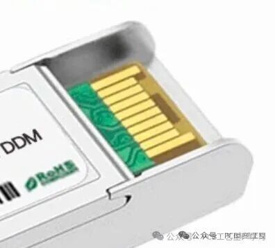
- Crosstalk Suppression Pressure: In high-density packages such as QSFP-DD, more than 120cm of wiring must be laid out per square centimeter, and the dense arrangement of 32 high-speed differential pairs and 8-channel optical fibers leads to a surge in crosstalk risk. Crosstalk in the 28GHz band must be controlled below -45dB to ensure signal quality.
(2) Physical Constraints of High-Density Integration
The trend towards miniaturization in optical module packaging (e.g., from QSFP to QSFP-DD) requires PCBs to achieve efficient integration of optoelectronic components within limited space, presenting dual challenges of spatial layout and manufacturing precision.
- Wiring Density Bottlenecks: 800G optical modules require line widths/spacing (L/S) of 20μm/20μm or even 15μm/15μm. Traditional subtractive processes lead to trapezoidal cross-sections due to the side-etching effect, making it easy to encounter broken lines or loss of precision when L/S is less than 40μm.
- Optoelectronic Synergy Conflicts: The 0°±0.5° positioning accuracy requirement of fiber arrays conflicts with the wiring needs of high-speed signal layers. Physical deformation of the fiber path can cause optical losses exceeding 0.5dB, while the electromagnetic field distribution of electrical channels may interfere with optical signal transmission.
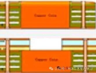
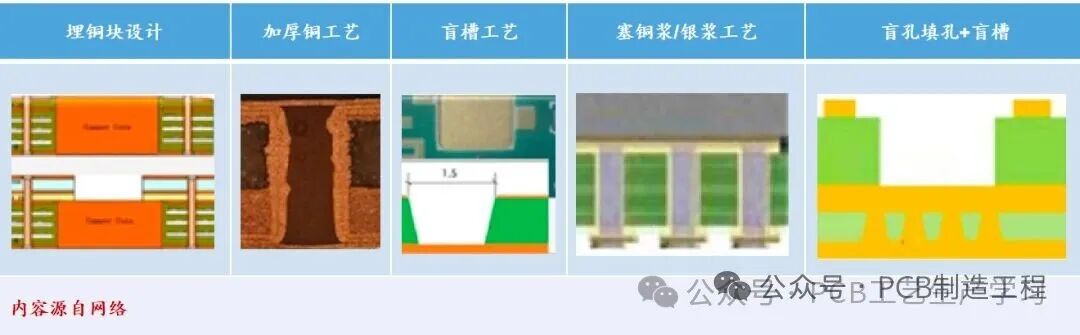
- Interlayer Interconnection Challenges: High-layer count PCBs (more than 20 layers) have become standard for Co-Packaged Optics (CPO) technology, requiring the diameter of blind/buried vias to be reduced to below 50μm while ensuring uniformity of copper thickness on the via walls, which traditional drilling and plating processes struggle to meet.
(3) Reliability Tests Under Extreme Environments
Optical modules are subjected to harsh environments of 85°C and 85% relative humidity in data centers for extended periods, posing severe challenges to the material stability and structural strength of PCBs.
- Thermal Matching Failure Risks: In CPO technology, the close integration of optical engines and chips leads to a sudden increase in PCB thermal flux density, requiring the substrate’s coefficient of thermal expansion (CTE) precision to reach ±0.8ppm/°C. If the CTE of the PCB does not match that of the silicon chip, stress cracking can occur during temperature cycling, leading to solder joint failures or line breaks.
- Material Aging Issues: High temperature and humidity environments accelerate hydrolysis of the PCB dielectric layer and corrosion of the copper layer. Variations in resin content in ordinary HDI boards can also cause dielectric constant drift, leading to decreased impedance stability, necessitating reliability testing for over 240 hours.
- Insufficient Heat Dissipation Capability: The power consumption of 400G optical modules has exceeded 10W, with 800G modules further increasing. Traditional aluminum heat sinks cannot quickly dissipate heat, and the thermal conductivity of PCBs, as a crucial component of the heat dissipation path, directly affects module lifespan.
(4) Balancing Process and Cost Challenges
The advanced technical requirements of optical modules drive process upgrades, but the cost pressures from high-end materials and precision manufacturing become bottlenecks for industrialization.
- Soaring Process Complexity: Advanced processes such as mSAP (Modified Semi-Additive Process) require high-end equipment like laser direct imaging (LDI) and horizontal pulse plating, with cleanliness requirements reaching Class 1000. The investment and operational costs of such equipment are significantly higher than those of ordinary HDI production lines.
- High Material Costs: Ultra-low loss substrates (e.g., Panasonic MEGTRON 8, Rogers RO3000 series) are 3-5 times the price of ordinary FR4, while the processing costs of ultra-low profile (HVLP) copper foil are also significantly higher than standard copper foil.
- Yield Control Difficulties: Pressing deviations in high-layer count PCBs, dust contamination of fine lines, and micron-level misalignment in optoelectronic alignment can all lead to decreased yield, further increasing unit costs.
2. Strategies and Breakthrough Directions for PCB Technology
To match the technological upgrades of optical modules, the PCB industry is undertaking systematic innovations from three dimensions: materials, processes, and design, forming a multi-level solution system.
(1) High-End Upgrades of Material Systems
Material innovation is the core to breaking through signal loss and reliability bottlenecks, forming a technological upgrade path around “low loss, high stability, strong thermal conductivity”.
- Ultra-Low Loss Dielectric Materials: Utilizing special substrates with Df values as low as 0.001~0.005, such as Isola Astra series and Shengyi Technology SU series, reduces dielectric loss by over 60% compared to traditional materials, combined with adjustable dielectric materials with Dk values of 3.8-4.6 to achieve dynamic impedance matching.
- High-Precision Conductor Materials: The widespread use of ultra-low profile (VLP) and HVLP copper foils minimizes surface roughness (Rz), reducing skin effect losses, while pulse plating technology achieves dense and uniform copper layers, enhancing signal transmission stability.
- Enhanced Thermal Management Materials: Development of metal-based composite substrates and ceramic-filled dielectric layers increases the thermal conductivity of PCBs from the traditional 0.3W/(m・K) to over 5W/(m・K), combined with embedded resistor/capacitor technology to reduce the number of heat-generating components.
(2) Precision Revolution in Manufacturing Processes
Processes are transitioning from “subtractive manufacturing” to “additive manufacturing”, breaking through the limits of miniaturization and high precision.
- Scaled Application of mSAP Technology: Achieving fine lines of 15μm/15μm through the process of “ultra-thin copper layer base – photosensitive dielectric forming – chemical copper plating – electroplating thickening – flash etching removal”, with standard rectangular cross-sections and impedance control precision improved to within ±3%.
- Deployment of High-End Equipment Clusters: Replacing contact exposure machines with laser direct imaging (LDI) equipment with precision below 5μm, combined with horizontal pulse plating and etching lines, ensures uniformity of line thickness and etching consistency, reducing process deviations.
- Breakthroughs in Heterogeneous Integration Processes: Developing direct bonding technology between indium phosphide lasers and silicon-based PCBs achieves seamless integration of optoelectronic devices, reducing interconnection losses, while machine vision-guided fiber positioning technology breaks alignment precision to ±0.1μm.
(3) Collaborative Innovation in Design Methods
Shifting from single circuit design to “electrical-optical-thermal” multi-physical field collaborative design, constructing a full-process optimization system.
- Three-Dimensional Layered Architecture Design: Adopting a layered strategy with a top layer for fiber arrays, a middle layer for high-speed signals, and a bottom layer for power control, achieving impedance transition between silicon photonic chips and PCBs through gradient microstrip line design (line width from 0.1mm to 0.15mm), reducing return loss by 8dB@56GHz.
- Application of Intelligent Routing Algorithms: Developing a three-dimensional obstacle avoidance engine based on an improved A* algorithm, combining the elastic mechanics model of fiber paths with electromagnetic field maps of electrical channels, dynamically planning routing paths, reducing routing completion time by 35%, while avoiding optoelectronic interference through the safety distance model D_min=0.3×λ_e + 0.7×R_f.
- Multi-Physical Field Simulation Optimization: Integrating signal integrity (SI), power integrity (PI), thermal simulation, and electromagnetic compatibility (EMC) simulation tools to predict losses, crosstalk, and thermal distribution during the design phase, optimizing heat dissipation structures and shielding designs in advance.
3. Future Evolution Trends of PCB Technology
As optical modules advance towards 1.6T and higher rates, coupled with the proliferation of new packaging technologies like CPO, PCBs will continue to evolve towards “optoelectronic integration, intelligent perception, and extreme performance”.
(1) Technical Dimension: From “Electrical Carrier” to “Optoelectronic Collaborative Platform”
PCBs will break through the traditional positioning of electronic circuit carriers, becoming the core hub for collaborative transmission of optoelectronic signals. Structurally, they will integrate functions such as microchannel cooling and embedded optical waveguides, achieving an integrated design of “circuit – optical path – thermal path”. In terms of materials, dynamically adjustable dielectric materials will achieve large-scale application, combined with self-healing resin-based materials to enhance module reliability in extreme environments. In terms of processes, development will move towards a mixed process of “semi-additive + 3D printing”, achieving precise manufacturing of micron-level lines and three-dimensional structures to meet the line precision requirements of 1.6T optical modules at 10μm/10μm.
(2) Application Dimension: CPO-Driven High-End Upgrades
CPO technology will accelerate breakthroughs in PCBs towards high layer counts, high density, and low loss. For AI server CPO optical engines, PCB layer counts will exceed 70 layers (e.g., NVIDIA GB200 uses a 70-layer substrate), while requiring dielectric loss (Df) to be below 0.0015 and the coefficient of thermal expansion control precision to be further improved to ±0.5ppm/°C. This trend will significantly enhance the value of high-end PCBs in optical modules, with the value of a single AI server PCB soaring from 5000 yuan in traditional servers to the million yuan level, creating structural market opportunities.
(3) Ecological Dimension: Intelligent Collaboration in Design and Manufacturing
The future PCB industry will build a full-chain intelligent ecosystem of “demand – design – manufacturing – testing”. On the design side, a virtual simulation platform will be constructed based on digital twin technology to achieve collaborative optimization of optical modules and PCBs; on the manufacturing side, AI visual inspection will replace manual inspections, improving defect identification accuracy to the nanometer level; on the testing side, an integrated optoelectronic testing system will be developed to simultaneously complete integrity testing of signals above 112Gbps and verification of optical coupling efficiency. At the same time, the industry will form unified design specifications and process standards to reduce adaptation costs for multi-vendor collaboration.
4. Conclusion
The iteration of optical module technology is the core driving force for the upgrade of the PCB industry. From 400G to 800G to 1.6T, each breakthrough is accompanied by systematic innovations in PCB materials, processes, and designs. Currently, the combination of mSAP technology and ultra-low loss materials has become standard for 800G optical modules, while the future proliferation of CPO technology will further drive PCBs towards higher precision, higher integration, and better performance. In this process, companies that can break through material bottlenecks, master core processes, and build collaborative design capabilities will gain competitive advantages, while the continuous advancement of PCB technology will provide critical support for the upgrade of global computing infrastructure.