Click the blue text to follow us
Follow and star our public account for exciting content delivered daily.

Source: Online materials
Many products in daily life, such as smartphones, digital cameras, and automotive cameras, feature CMOS Image Sensors (CIS). With their help, people can obtain clearer and higher-quality images and videos. This is mainly due to the fact that CMOS image sensors are devices that convert light into electrical signals, and with advancements in CMOS process technology, these sensors, acting as the “eyes” of cameras, have achieved high resolution, low noise, a wide dynamic range, and intelligent features.
So, do you know how CMOS image sensors have evolved to their current state? What classifications do they have? This article will take you through the evolution of CMOS image sensors, as well as the advantages and applicable scenarios of stacked versus monolithic technologies.
The Development History of CMOS Image Sensors
Since the invention of the Charge-Coupled Device (CCD) by Bell Labs in 1969 and the introduction of the concept of solid-state imaging devices, solid image sensors have rapidly developed, becoming an important branch of sensing technology. In fact, the research on Complementary Metal-Oxide-Semiconductor (CMOS) image sensors began almost simultaneously with that of CCD image sensors. However, due to the limitations of the technology at the time, CMOS image sensors suffered from poor image quality, low resolution, high noise, and insufficient light sensitivity, which led to a lack of attention and development.
Later, with advancements in integrated circuit (IC) design technology and process levels, the previous shortcomings of CMOS image sensors were overcome, and they gradually became a research hotspot and the mainstream in the market.
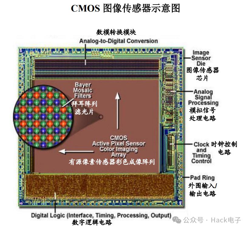
Figure: Schematic diagram of the internal structure of a CMOS image sensor (Source: Geke Micro’s prospectus)
The greatest advantage of CMOS image sensors is their ability to be integrated onto a single chip, allowing for the integration of image sensing and acquisition, analog signal processing circuits, analog-to-digital conversion modules, digital logic circuits, clock control circuits, and peripheral input/output circuits all on one chip. The working principle is that the light-sensitive unit array first converts the brightness and color information of the captured scene from light signals into electrical signals; then the electrical signals are read out and converted into digital signals through the ADC module; finally, the digital signals are pre-processed and transmitted to the platform for reception via a transmission interface.
The birth of CMOS image sensors has two versions. One was developed in April 1993 by Dr. Eric R. Fossum’s team at NASA’s Jet Propulsion Laboratory (JPL), which created the CMOS active pixel sensor. However, the response from NASA was not optimistic, so in 1995, Fossum, along with his then-wife and colleague Sabrina Kemeny, founded Photobit to commercialize CMOS sensors. They launched their first product, the PB-159, in 1998, followed by the PB-100 the next year, which was used in Intel’s Easy PC camera, bringing video conferencing into the workplace.
The other version was published in a paper in 1989 by Professor Peter Denyer and Dr. David Renshaw from the University of Edinburgh, along with researchers Wang Guoyu and Lu Mingying, who were working at the university. They introduced their research on CMOS image sensors and successfully produced a chip by the end of 1990.
Regardless of which version, both were submerged in the market’s tide, and today, the leading players in the CMOS image sensor market are mainly Sony, Samsung Electronics, and Geke Micro.
Classification of CMOS Image Sensors
CMOS image sensors can be mainly classified based on the position of the light-sensitive elements into Front-Side Illuminated (FSI), Back-Side Illuminated (BSI), and the improved Stacked structure based on BSI.
Early CMOS image sensors were primarily of the FSI structure due to its simple manufacturing process; however, its disadvantage is that because the light-sensitive elements are on the bottom layer, the amount of incoming light is limited, resulting in average imaging quality. The pixel range for this type of CMOS image sensor is generally below 2 million pixels.
To enhance overall imaging quality, the BSI structure emerged, which changed the direction of light incidence, separating electrical components from light, effectively reducing photon loss and significantly improving the quantum efficiency of CMOS image sensors, enhancing photo quality in low-light and outdoor scenarios. In other words, compared to the FSI structure, it has higher sensitivity and quantum efficiency, a wider light-sensitive angle, lower pixel crosstalk, and better imaging quality, but its complexity and cost are higher. This structure is mainly used in CMOS image sensor products with over 5 million pixels.
In fact, Geke Micro, established in 2003, began researching CMOS image sensors early on and successfully developed the first domestic FSI structure CMOS image sensor in 2005; in 2012, they achieved a technological breakthrough and launched the first domestic BSI image sensor.
As market demands for pixel count, frame rate, and imaging quality (such as high signal-to-noise ratio, low light, and dynamic environment perception) continue to rise, Sony developed the Stacked structure based on BSI, retaining only the light-sensitive elements on the upper layer while moving all the wiring layers to the lower layer of the light-sensitive elements, stacking the two layers of chips together. This significantly reduces the overall chip area and effectively suppresses circuit noise, resulting in better light-sensitive performance. The Stacked CMOS image sensors can increase the area ratio of the pixel layer in the sensing unit from nearly 60% in traditional designs to nearly 90%, greatly optimizing image quality. Similarly, to achieve the same image quality, the physical size of Stacked CMOS image sensors can be significantly reduced compared to other types of CMOS image sensors. This has improved the cost structure of CMOS image sensors, gradually making them the mainstream in the high-pixel CMOS market.
However, in recent years, another high-pixel CIS technology route has emerged in the industry, which is distinctly different from the Stacked structure—monolithic high-pixel integration.
Geke Micro’s Monolithic High-Pixel Technology
To meet the market’s demand for high-pixel, high-frame-rate, and high-quality imaging in CMOS image sensors, Geke Micro has taken a different approach. Leveraging nearly 20 years of experience in single-layer wafer CMOS technology, they independently developed monolithic high-pixel processes and circuit technologies, overcoming the compatibility gap between pixel-specific processes and conventional logic processes, achieving high-quality imaging without stacking.
For example, Geke Micro has implemented its proprietary technology—FPPI (Floating Poly Pixel Isolation) isolation technology, which achieves high pixel counts while reducing the sources of white spots and dark current, ensuring imaging quality. The performance of the GC32E1 image sensor, which uses this patented technology with 0.7μm pixels, exemplifies this. This high-pixel monolithic CMOS image sensor matches the performance of stacked products in various imaging metrics.
According to publicly available information, the GC32E1 supports 32 million full-pixel output and, when paired with the Remosaic decoding function on mobile platforms, can produce photos with rich details and vibrant colors. Even in nighttime or low-light environments, it can capture bright and clear images. Moreover, in video applications, it supports interleaved HDR technology, enhancing dynamic range in environments with significant light-dark differences, preventing dark areas from appearing black or bright areas from being overexposed.
It is worth mentioning that Geke Micro has also innovated in the design of on-chip ADC circuits, digital circuits, and interface circuits, allowing its monolithic high-pixel CMOS image sensors to be compatible with the module sizes of dual-chip stacked products on the market, with only about a 10% increase in area, while reducing total silicon wafer usage by 40%, significantly improving wafer area utilization and greatly enhancing cost structure.
Currently, Geke Micro’s CMOS sensor products utilizing FPPI technology include GC50B2, GC50E0, GC32E1, GC08A3, GC13A0, GC13A2, GC16B3, etc. Among them, the monolithic 32 million pixel CIS has been introduced to brands and successfully mass-produced, validating the feasibility and mass production capability of the monolithic technology route. It is reported that Geke Micro will continue to launch high-pixel specifications of 50 million and above based on the monolithic high-pixel platform in the future.
Conclusion
Monolithic CMOS image sensors and Stacked CMOS image sensors are currently two widely used technologies in image sensing technology, each with its applicable scenarios and limitations. In the high-pixel domain, thanks to advancements in processes and technologies, the advantages of monolithic CIS are becoming increasingly apparent, and it may become as important a technology route as Stacked. In the future, as the mobile imaging and other terminal markets mature, and with the continuous development of technologies such as artificial intelligence and cloud computing, CMOS image sensors will continue to upgrade, with more innovations and applications emerging.

Want to learn about FPGA? Here are some examples, ZYNQ design, follow our public account to explore.