Data Input Stage
1. Check if the received data in the process is complete (including: schematic, *.brd file, bill of materials, PCB design specifications, and PCB design or modification requirements, standardization requirements, process design specification documents).
2. Confirm that the PCB template is the latest version.
3. Verify that the positioning of components in the template is correct.
4. Ensure that the PCB design specifications and PCB design or modification requirements, standardization requirements are clear.
5. Confirm that the prohibited placement areas and routing zones on the outline diagram are reflected in the PCB template.
6. Compare the outline diagram to ensure that the dimensions and tolerances marked on the PCB are correct, and that the definitions of metallized and non-metallized holes are accurate.
7. After confirming that the PCB template is accurate, it is best to lock the structural file to prevent accidental movement.
Post-Layout Check Stage
Component Check
1. Confirm that all component packages are consistent with the company’s unified library and that the package library has been updated (check the results using viewlog). If they are inconsistent, be sure to update symbols.
2. For motherboards and daughter boards, single boards and backplanes, confirm that signals correspond, positions correspond, connector orientations and silkscreen markings are correct, and that daughter boards have anti-insertion measures. Components on the daughter board should not interfere with those on the mother board.
3. Ensure that components are 100% placed.
4. Open the place-bound for the TOP and BOTTOM layers of components and check if the DRC caused by overlaps is permissible.
5. Ensure that the marking points are sufficient and necessary.
6. Heavier components should be placed near the PCB support points or edges to reduce PCB warping.
7. After placing components related to the structure, it is best to lock them to prevent accidental movement.
8. Within a 5mm range around the press-fit socket, no components exceeding the height of the press-fit socket are allowed on the front, and no components or solder points are allowed on the back.
9. Confirm that the component layout meets process requirements (focus on BGA, PLCC, and surface mount sockets).
10. For components with metal housings, pay special attention to ensure they do not collide with other components and leave enough space.
11. Interface-related components should be placed as close to the interface as possible, and backplane bus drivers should be placed as close to the backplane connectors as possible.
12. Confirm that chip components on the wave soldering surface have been converted to wave soldering packages.
13. Ensure that the number of manual solder points does not exceed 50.
14. For components with high axial insertion on the PCB, consider horizontal installation. Leave space for horizontal placement and consider fixing methods, such as the fixing pads for oscillators.
15. For components that require heat sinks, confirm that there is enough distance from other components and pay attention to the height of major components within the heat sink range.

Function Check
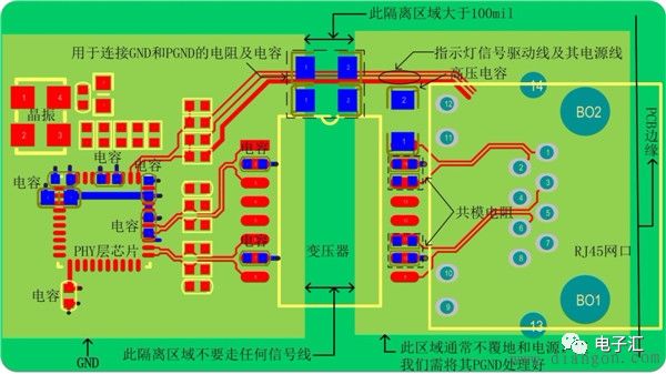
1. For mixed-signal boards, confirm that the digital and analog circuit components are separated, and that the signal flow is reasonable.
2. Place the A/D converter across the analog-digital partition.
3. Check if the layout of clock components is reasonable.
4. Check if the layout of high-speed signal components is reasonable.
5. Ensure that termination components are placed reasonably (source matching series resistors should be placed at the signal driving end; intermediate matching series resistors should be placed in the middle; terminal matching series resistors should be placed at the signal receiving end).
6. Check if the number and position of decoupling capacitors for IC components are reasonable.
7. Signal lines should use different voltage planes as reference planes, and when crossing plane split areas, the connection capacitance between reference planes should be close to the signal routing area.
8. Check if the layout of protection circuits is reasonable and conducive to segmentation.
9. The fuse for the single board power supply should be placed near the connector, with no circuit components in front of it.
10. Confirm that strong signals and weak signals (with a power difference of 30dB) are routed separately.
11. Ensure that components that may affect EMC testing are placed according to design guidelines or successful reference experiences. For example, the reset circuit on the panel should be placed close to the reset button.
Heat Generation
1. Heat-sensitive components (including liquid medium capacitors, oscillators) should be kept as far away as possible from high-power components, heat sinks, and other heat sources.
2. Check if the layout meets thermal design requirements and if the heat dissipation channels are executed according to the process design documents.
Power Supply
1. Check if the IC power supply is too far from the IC.
2. Check if the layout of the LDO and surrounding circuits is reasonable.
3. Check if the layout of module power supplies and surrounding circuits is reasonable.
4. Check if the overall layout of the power supply is reasonable.
Rule Settings
1. Confirm that all simulation constraints have been correctly added to the Constraint Manager.
2. Confirm that physical and electrical rules are set correctly (pay attention to the constraint settings for power and ground networks).
3. Check if the spacing settings for Test Via and Test Pin are sufficient.
4. Check if the thickness and scheme of the stack meet design and processing requirements.
5. Confirm that all differential lines with characteristic impedance requirements have been calculated and controlled by rules.
Post-Wiring Check Stage
Digital and Analog
1. Check if the routing of digital circuits and analog circuits has been separated and if the signal flow is reasonable.
2. If A/D, D/A, and similar circuits have split grounds, check if the signal lines between the circuits run from the bridging points between the two grounds (differential lines are exceptions).
3. Signal lines that must cross the gaps between split power supplies should reference a complete ground plane.
4. If using ground layer design without segmentation, ensure that digital and analog signals are routed separately.
Clock and High-Speed Sections
1. Check if the impedance of high-speed signal lines is consistent across layers.
2. For high-speed differential signal lines and similar signal lines, ensure they are of equal length, symmetrical, and routed nearly parallel.

3. Confirm that clock lines are routed as much as possible on inner layers.
4. Confirm that clock lines, high-speed lines, reset lines, and other strongly radiating or sensitive lines are routed according to the 3W principle as much as possible.
5. Ensure that there are no branching test points on clock, interrupt, reset signals, 100M/1G Ethernet, and high-speed signals.
6. Ensure that low-level signals like LVDS and TTL/CMOS signals meet the 10H requirement (H is the height of the signal line from the reference plane).
7. Ensure that clock lines and high-speed signal lines avoid crossing dense via areas or routing between component pins.
8. Ensure that clock lines meet SI constraints (clock signal routing should minimize vias, be short, and have continuous reference planes, with the main reference plane ideally being GND; if the reference plane changes when switching layers, there should be GND vias within 200 mil of the vias; if the reference plane changes to a different level, there should be decoupling capacitors within 200 mil of the vias).
9. Ensure that differential pairs, high-speed signal lines, and various buses meet SI constraints.
EMC and Reliability
1. For oscillators, ensure that a ground layer is placed underneath; avoid routing signal lines between component pins; for high-speed sensitive components, avoid routing signal lines between component pins.
2. There should be no sharp angles or right angles on the signal routing lines (generally, use continuous 135-degree turns; RF signal lines should preferably use arcs or calculated chamfered copper foil).
3. For double-sided boards, check if high-speed signal lines are routed closely alongside their return ground lines; for multilayer boards, check if high-speed signal lines are routed as close to the ground plane as possible.
4. For adjacent signal routing lines on two layers, try to route them vertically.
5. Avoid routing signal lines under power modules, common mode inductors, transformers, and filters.
6. Try to avoid long-distance parallel routing of high-speed signals on the same layer.
7. Check if the edges of digital ground, analog ground, and protective ground at the board edges have shielding vias; check if multiple ground planes are connected with vias; ensure that the distance between vias is less than 1/20 of the wavelength of the highest frequency signal.
8. Ensure that the signal routing lines corresponding to surge suppression devices are short and thick on the surface layer.
9. Confirm that the power and ground layers have no islands, no excessive slots, no long ground plane cracks caused by oversized or dense vias, and no narrow strips and channels.
10. Ensure that ground vias are placed in areas where signal lines cross multiple layers (at least two ground planes are needed).
Power and Ground
1. If the power/ground plane is split, try to avoid crossing high-speed signals over the split reference plane.
2. Confirm that the power and ground can carry sufficient current. Check if the number of vias meets the carrying requirements (estimation method: for outer layer copper thickness of 1oz, 1A/mm line width; for inner layer, 0.5A/mm line width; double the current for short lines).
3. For power supplies with special requirements, confirm that the voltage drop requirements are met.
4. To reduce the radiation effect of the plane edges, try to meet the 20H principle between the power layer and ground layer (if conditions allow, the more the power layer is recessed, the better).
5. If there is a ground split, ensure that the split ground does not form a loop.
6. Ensure that adjacent layers with different power planes avoid overlapping placement.
7. Ensure that the isolation between protective ground, -48V ground, and GND is greater than 2mm.
8. Ensure that -48V ground is only for -48V signal return and does not connect to other grounds; if this is not possible, please explain the reason in the remarks.
9. Near the connector panel, ensure that there is a protective ground of 10~20mm, connected with staggered double-row vias.
10. Check if the spacing between power lines and other signal lines meets safety regulations.
Forbidden Routing Areas
1. Under metal housing components and heat sinks, there should be no routing, copper foil, or vias that could cause short circuits.
2. Around installation screws or washers, there should be no routing, copper foil, or vias that could cause short circuits.
3. Check if there are any routing in reserved positions as per design requirements.
4. The spacing between non-metallized holes and inner layer routing and copper foil should be greater than 0.5mm (20mil), and for outer layers, it should be greater than 0.3mm (12mil); for single board puller shaft holes, the spacing should be greater than 2mm (80mil).
5. The recommended distance from copper foil and lines to the board edge should be greater than 2mm, with a minimum of 0.5mm.
6. The distance from inner layer ground copper foil to the board edge should be 1~2mm, with a minimum of 0.5mm.
Pad Outlines
1. For chip components with two pads (0805 and below), such as resistors and capacitors, the printed lines connecting to their pads should ideally be symmetrically routed from the center of the pads, and the printed lines connecting to the pads must have the same width. For lines with widths less than 0.3mm (12mil), this rule can be disregarded.
2. For pads connected to wider printed lines, it is best to transition through a narrow printed line (for 0805 and below).
3. Lines should ideally be routed from both ends of the pads of devices like SOIC, PLCC, QFP, SOT.
Silkscreen
1. Check if any component designators are missing and if the positions can correctly identify the components.
2. Check if the component designators meet company standards.
3. Confirm the correctness of the pin arrangement, pin 1 marking, polarity marking, and connector orientation marking of the components.
4. Check if the insertion direction markings of the mother board and daughter board correspond.
5. Check if the backplane correctly marks the slot names, slot numbers, port names, and sheath directions.
6. Confirm that the silkscreen additions required by the design are correct.
7. Confirm that there are anti-static and RF board markings (for RF boards).
Barcodes
1. Confirm that the PCB coding is correct and meets company specifications.
2. Confirm that the PCB coding position and layer for the single board are correct (should be in the upper left corner of side A, on the silkscreen layer).
3. Confirm that the PCB coding position and layer for the backplane are correct (should be in the upper right corner of side B, on the outer copper foil surface).
4. Confirm that there is a laser-printed white silkscreen marking area for the barcode.
5. Confirm that there are no connections or vias larger than 0.5mm under the barcode frame.
6. Confirm that there are no components exceeding 25mm in height within a 20mm range outside the white silkscreen area of the barcode.
Vias
1. On the reflow soldering surface, vias should not be designed on pads (the distance between open-window vias and pads should be greater than 0.5mm (20mil), and the distance between green oil-covered vias and pads should be greater than 0.1mm (4mil); method: turn off Same Net DRC, check DRC, then turn Same Net DRC back on).
2. The arrangement of vias should not be too dense to avoid causing large-scale breaks in power and ground planes.
3. The diameter of drilled vias should preferably not be less than 1/10 of the board thickness.
Process
1. Check if the component placement rate is 100% and if the connectivity rate is 100% (if not reaching 100%, it needs to be explained in the remarks).
2. Ensure that dangling lines have been minimized, and that retained dangling lines have been confirmed one by one.
3. Check if the process issues reported by the process department have been carefully verified.
Large Area Copper Foil
1. For large area copper foil on the top and bottom, unless there are special needs, use grid copper (use diagonal grid for single boards, orthogonal grid for backplanes, with line width of 0.3mm (12 mil) and spacing of 0.5mm (20mil)).
2. The pads of components in large area copper foil zones should be designed as flower pads to avoid cold solder joints; if there are current requirements, consider widening the flower pad ribs first, then consider full connection.
3. When applying large area copper, try to avoid dead copper (islands) that are not network connected.
4. Large area copper foil should also pay attention to illegal connections and unreported DRCs.
Test Points
1. Ensure that there are sufficient test points for various power and ground (at least one test point for every 2A of current).
2. Confirm that networks without test points are confirmed to be reducible.
3. Confirm that no test points are set on components that are not installed during production.
4. Ensure that Test Via and Test Pin are fixed (applicable to modified boards where the test pin bed does not change).
DRC
1. The spacing rule for Test Via and Test Pin should first be set to the recommended distance, check DRC, and if there are still DRCs, then check DRC with the minimum distance setting.
2. Open the constraint settings to an open state, update DRC, and check if there are any disallowed errors in the DRC.
3. Confirm that DRC has been minimized, and for those that cannot be eliminated, confirm them one by one.
Optical Reference Points
1. Confirm that the PCB surface with mounted components has optical reference symbols.
2. Confirm that the optical reference symbols do not overlap with lines (silkscreen and copper foil routing).
3. The background of optical reference points should be the same, and confirm that the optical points on the entire board have their centers at least 5mm from the edges.
4. Confirm that the optical reference baseline symbols on the entire board have assigned coordinate values (it is recommended to place the optical reference baseline symbols as components), and that they are integer values in millimeters.
5. For ICs with pin centers <0.5mm and for BGAs with center distances less than 0.8mm (31 mil), optical reference points should be set near the diagonal positions of the components.
Solder Mask Check
1. Confirm that any special requirement types of pads are correctly opened (especially pay attention to hardware design requirements).
2. Check if the vias under the BGA are treated as covered oil plug holes.
3. Confirm that vias other than test vias have been opened as small windows or covered oil plug holes.
4. Ensure that the opening of optical reference points avoids exposing copper and lines.
5. For power chips, oscillators, and other devices that require copper foil for heat dissipation or grounding shielding, ensure that there is copper foil and that it is correctly opened. Devices fixed by solder should have green oil to block the large-area diffusion of solder.
Output Processing Files
Drilling Diagram
1. Check if the notes on PCB thickness, number of layers, silkscreen color, warpage, and other technical specifications are correct.
2. Check if the layer names, stacking order, dielectric thickness, and copper foil thickness in the stacking diagram are correct; check if impedance control is required and if the description is accurate; ensure that the layer names in the stacking diagram match their photoplot file names.
3. Turn off the Repeat code in the settings table, and set the drilling accuracy to 2-5.
4. Ensure that the hole table and drilling files are up to date (when changing holes, they must be regenerated).
5. Check if there are any abnormal hole diameters in the hole table, and if the hole diameters for press-fit components are correct; ensure that the hole diameter tolerances are correctly marked.
6. Ensure that vias that need to be filled are listed separately and marked as “filled vias”.
Photoplot
1. Photoplot files should preferably be output in RS274X format, and the accuracy should be set to 5:5.
2. Check if art_aper.txt is up to date (274X may not be needed).
3. Check if there are any abnormal reports in the log file of the output photoplot files.
4. Confirm the edges and islands of the negative layers.
5. Use photoplot inspection tools to check if the photoplot files match the PCB (for modified boards, use comparison tools for comparison).
File Completeness
1. PCB file: product model_specification_single board code_version.brd
2. Backplane substrate design file: product model_specification_single board code_version-CB[-T/B].brd
3. PCB processing files: PCB code.zip (including photoplot files for each layer, aperture table, drilling files, and ncdrill.log; for panelized boards, also include the panel file provided by the process *.dxf), backplane should also include substrate files: PCB code-CB[-T/B].zip (including drill.art, *.drl, ncdrill.log).
4. Process design file: product model_specification_single board code_version-GY.doc
5. SMT coordinate file: product model_specification_single board code_version-SMT.txt (when outputting coordinate files, confirm to select Body center; only select Symbol origin when confirming that all SMD component libraries have their origins at the component center).
6. PCB structural file: product model_specification_single board code_version-MCAD.zip (including .DXF and .EMN files provided by structural engineers).
7. Test files: product model_specification_single board code_version-TEST.ZIP (including testprep.log and untest.lst or *.drl test point coordinate files).
8. Archived drawing files: product model specification-single board name-version.pdf (including: cover, first page, silkscreen for each layer, routing for each layer, drilling diagram, backplane including substrate diagram).
Standardization
1. Confirm that the information on the cover and first page is correct.
2. Confirm that the drawing serial numbers (corresponding to the PCB layer order) are correct.
3. Confirm that the PCB code on the drawing frame is correct.
Disclaimer:This article’s material is sourced from the internet, and the copyright belongs to the original author. If there are any copyright issues, please contact me for removal.
 |
Share electronic-related technical articles, news, and communication meetings. Subtle progress every day. Gathering electronic technology. |