Like many other great inventions in history, the printed circuit board (PCB) as we know it today is built on the foundation of historical advancements. In our little corner of the world, we can trace the history of PCBs back over 130 years, when the great industrial machines of the world were just beginning to operate. What we will introduce in this blog is not a complete history but important moments that transformed PCBs into what they are today.
Why PCBs?
Over time, PCBs have evolved into tools that optimize the manufacturing of electronic products. What was once easy to assemble by hand quickly gave way to microscopic components that require mechanical precision and efficiency. The two circuit boards shown below serve as examples. One is an old board made for calculators in the 1960s. The other is a typical high-density motherboard that you would see in today’s computers.
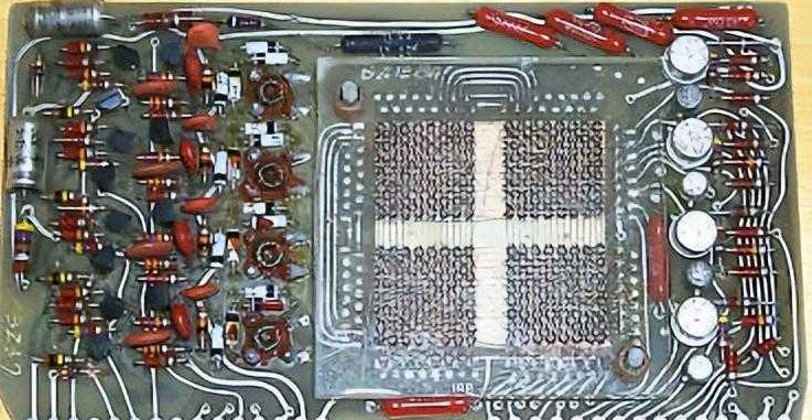
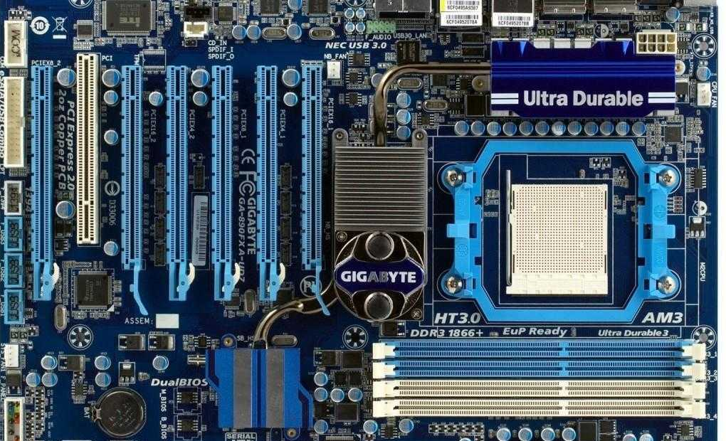
Comparison of PCBs between the 1968 calculator and today’s modern motherboard. (Image 1 source, Image 2 source)
In calculators, we might have over 30 transistors, but on a single chip on a motherboard, you can find over a million transistors. The point is that the pace of advancement in technology and PCB design itself is impressive. Now, everything that was on the calculator PCB can fit into a single chip designed today. This brings attention to several significant trends in PCB manufacturing:
-
We are integrating more functions into advanced devices like integrated circuits (ICs) and microprocessors.
-
We are shrinking passive components such as resistors and capacitors down to microscopic levels.
-
All of this has led to increased component density and complexity on our circuit boards.
All these advancements are primarily driven by the increased speed and functionality of our products. We want our devices to respond immediately; even a few seconds of delay can drive us crazy. For functionality, consider video games. Back in the 80s, you were likely playing Pac-Man in an arcade. Now we are seeing photo-realistic representations. The progress is astounding.

Today, the visuals of video games are nearly realistic.
It is clear that the development of PCBs is a direct response to our expectations of devices. We need faster, cheaper, and more powerful products, and the only way to meet these demands is to miniaturize the manufacturing process and improve efficiency. When did this surge of electronics and PCBs begin? At the dawn of the Gilded Age.
The Gilded Age (1879 – 1900)
We ended the Civil War in the 60s, and now American manufacturing is booming. During this time, we are doing everything we can, from food to clothing, furniture, and railroads. The transportation industry is making a major advance, and our greatest engineers are exploring how to get someone from the East Coast to the West Coast in 5 to 7 days instead of 5 to 7 months.
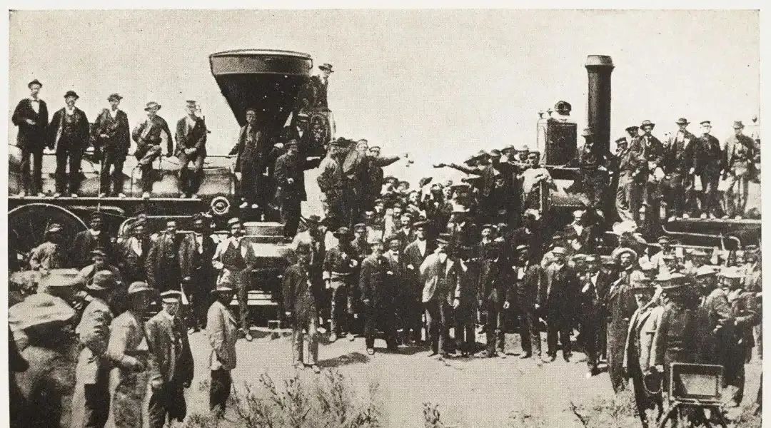
Railroads made travel from the East Coast to the West Coast take only days instead of months.
During this time, we also introduced electricity into homes, starting first from cities and then into suburbs and rural areas. Electricity is now a substitute for coal, wood, and oil. Imagine living in New York during a harsh winter, trying to cook or heat with dirty coal or piles of firewood. Electricity changed all of that.
An interesting question is that the Standard Oil Company, which monopolized the oil market, did not supply oil for gasoline. Their market was oil for cooking, frying, and lighting. With the advent of electricity, Standard Oil needed to define a new use for oil, which would come with the launch of automobiles.
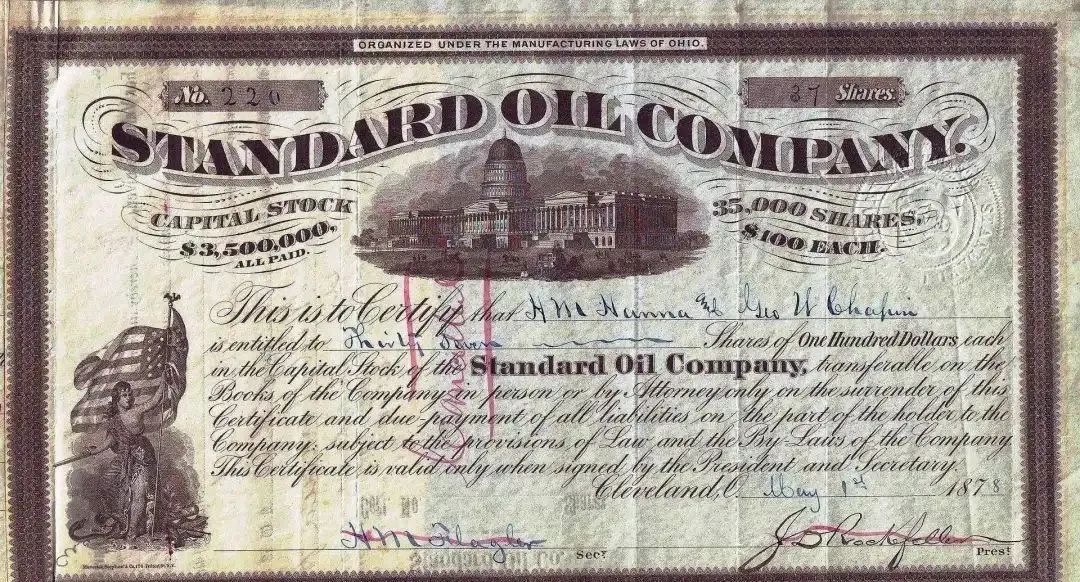
In May 1878, the Standard Oil Company issued stock, marking the beginning of the oil monopoly.
During the Gilded Age, we saw some major discoveries in electromagnetism. We invented the electric motor, which converts electrical energy into mechanical energy. We also saw the generator, which does the opposite by converting mechanical energy into electrical energy.
This was also a time of brilliant inventors whose innovations still affect our electronic world today, including:
-
Thomas Edison invented the light bulb in 1879, the movie in 1889, and many other innovations.
-
Nikola Tesla invented the electric motor in 1888 and AC power in 1895.
-
Alexander Graham Bell invented the telephone in 1876.
-
George Eastman’s Kodak invented the first consumer camera in 1884.
-
Herman Hollerith invented the tabulating machine in 1890, which later founded IBM.
During this intense period of innovation, one of the biggest debates was between alternating current (AC) and direct current (DC). Tesla’s AC eventually became the ideal method for long-distance power transmission. However, interestingly, we are still dealing with the AC-DC conversion issue today.
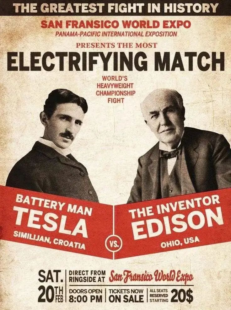
AC may have won this battle, but DC still dominates electronic products.
Look at any electronic device you plug into the wall, you need to convert AC to DC. Or, if you look at the infrastructure needed for solar panels, they generate power in DC, which must be converted back to AC as power, and then converted back to DC for our devices. You could almost say the AC-DC debate has never ended; just a balance has been struck between the two opposing ideas.
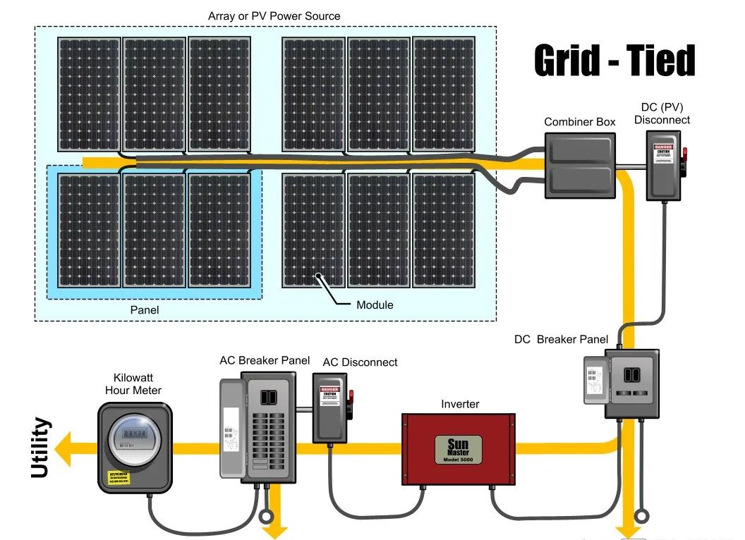
There is a lot of back and forth between AC and DC in solar panels.
Note that the original idea of PCBs was not invented during the Gilded Age. However, without the manufacturing capabilities of this era and the widespread influence of electricity, PCBs would never have become what they are today.
The Progressive Era (1890 – 1920)
The Progressive Era is marked by a period of social reform, with legislation like the Sherman Antitrust Act breaking the monopoly of Standard Oil. This was also when we saw the first PCB patent. In 1903, German inventor Albert Hanson applied for a British patent for a device described as a flat foil conductor on a multilayer insulated board. Sound familiar?
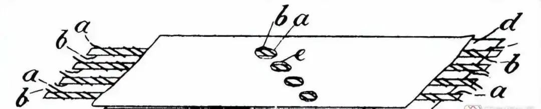
Diagram depicting the first PCB patent obtained by Albert Hanson.
Hanson also described the concept of via applications in his patent. Here, he demonstrated that you could drill a hole in two layers with vertical lines to establish electrical connections.
During this time, we began to see Edison and other business leaders pushing electrical devices into everyday homes. The problem with this push was the complete lack of standardization. If you lived in New York or New Jersey and used Edison’s electrical inventions for lighting, heating, or cooking, what would happen if you used them in another city? They wouldn’t work because each town had its own socket configuration.
Edison not only wanted to sell people a light bulb, but he also wanted to sell a service, which made the problem worse. Edison could provide you with electricity service monthly; then you would purchase light bulbs, appliances, etc. Of course, these services were not compatible with other competing methods.
We owe it to Harvey Hubbel for finally ending this chaos. In 1915, he patented the standard wall outlet plug still in use today. Now we don’t plug in toasters or heating pads into light bulb sockets. This was a huge victory for industry standardization.
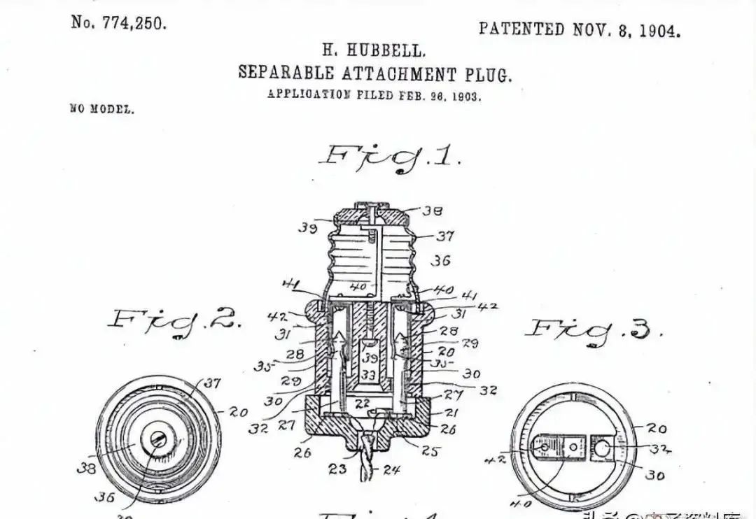
Thanks to Harvey Hubbel, we now have a standardized wall outlet for all electronic devices.
It’s worth noting that the Progressive Era also marked the First World War. This conflict was purely focused on mechanical devices and trench warfare. The concept of PCBs and even basic electronic products had not yet been used for military applications, but would soon be.
The Roaring Twenties (1920s)
With the end of the First World War, we are now in the Roaring Twenties, witnessing a huge prosperity in the American economy. For the first time in history, more people lived in cities than on farms. We also began to see the introduction of chains and brands across the United States. You might have a family store in two different towns, but now we have major brands and stores going nationwide.
The greatest invention of this period was Henry Ford’s automobile and the infrastructure it required. This is similar to the 1990s when we had to establish a major infrastructure by building switches, routers, and fiber optics to handle the internet and our information age. The automobile was no exception.
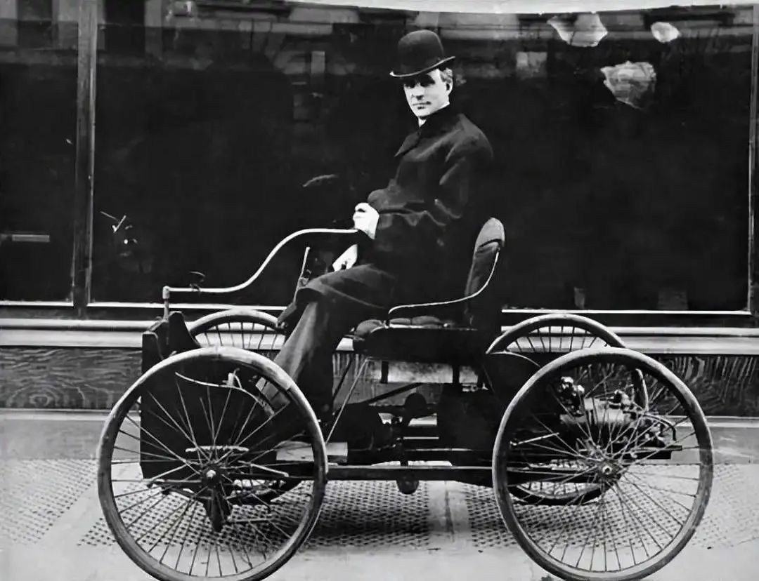
Henry Ford’s first car—the Quadricycle.
Here we see once muddy roads being paved. People needed gasoline to power their vehicles, leading to the emergence of gas stations. You also had repair shops, parts, etc. Many people’s entire way of life stemmed from the invention of the automobile, and it still does today.
It was also during this time that we saw the introduction of modern appliances we still rely on today, such as washing machines, vacuum cleaners, and refrigerators. This was the first time people could buy perishable goods in stores and store them to extend freshness.
But where are our PCBs? We still don’t see them in any appliances or cars launched during this period. However, in 1925, Charles Ducas submitted a patent that described the process of adding conductive ink to insulating materials. This would later produce printed wiring boards (PWB). This patent was the first practical application similar to PCBs, but only used as flat heating coils. We still hadn’t achieved any actual electrical connections between circuit boards and components, but we were getting close.
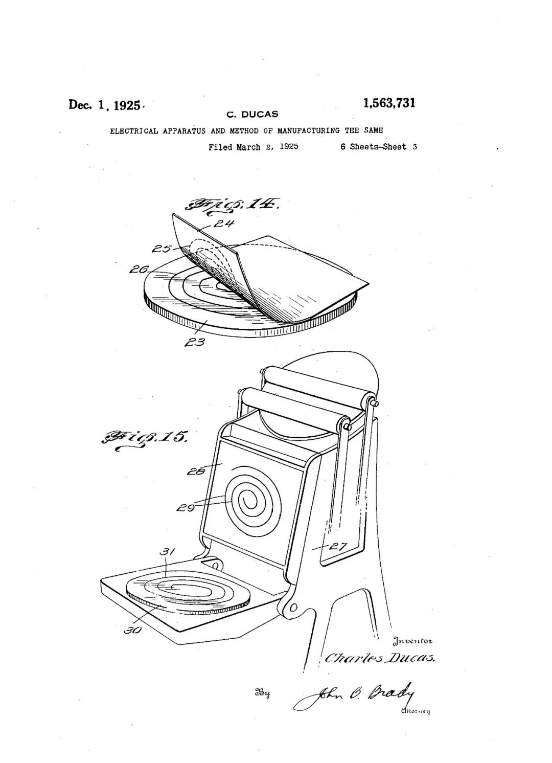
PCBs continued to evolve, this time being used as heating coils by Charles Ducas.
The Great Depression (1930s)
In 1929, the stock market crashed, and all the great innovations of our time fell flat. Here we see a period where unemployment exceeded 25%, 25,000 banks failed, and massive hardships rippled across the globe. It was a tragic time for humanity, paving the way for the rise of Hitler, Mussolini, Stalin, and the world conflicts that would follow. Until now, PCBs may have remained silent, but all that was about to change.
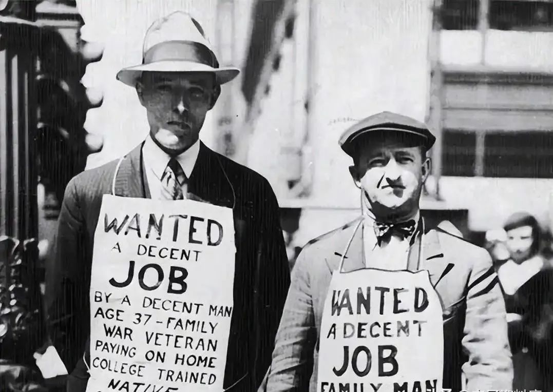
The Great Depression affected everyone, from banks to ordinary workers.
World War II (1939 – 1945)
World War II was underway, and America joined the fight after the Pearl Harbor attack in 1942. The interesting thing about the Pearl Harbor incident was the entire communication failure that led to the attack. The U.S. had ample evidence that a crisis was imminent, but all communication with their military base in Honolulu failed, leaving the island caught off guard.

A battleship that went missing during the Pearl Harbor attack.
Due to this failure, the U.S. Department of Defense realized they needed a more reliable means of communication. This brought electronics to the forefront as a primary means of communication, replacing Morse code.
Also during World War II, we saw the first use of PCBs in proximity fuses. This device was used for high-speed projectiles that required long-distance precision targeting in the air or on land. The proximity fuse was initially developed by the British to counter the advance of Hitler’s army, later shared with the U.S. for design and manufacturing refinement.
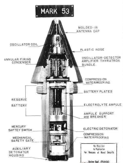
One of the first military applications of PCBs—the proximity fuse.
During this time, we also had the Austrian Paul Eisler residing in the UK who patented copper foil on non-conductive glass substrates. Sound familiar? This is the concept we still use today for manufacturing PCBs with an insulating layer and copper on the top/bottom. Eisler made a radio with his PCB in 1943, which paved the way for future military applications.
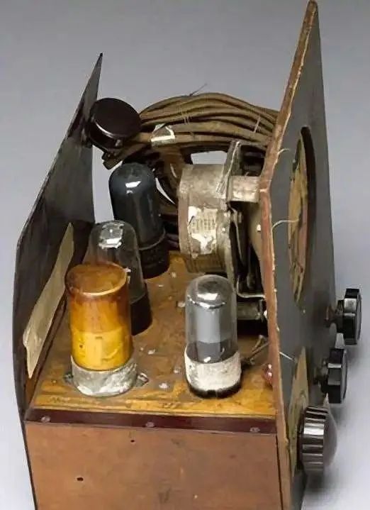
Paul Eisler’s radio made with the first printed circuit board (PCB).
The Baby Boom Generation (1940s)
As World War II came to a close, we saw our soldiers returning home, starting families, and having a bunch of children. Enter the Baby Boom Generation. It was in the post-war era that we saw a massive improvement in existing appliances like vacuum cleaners, washing machines, televisions, and radios. Now that the Great Depression was over, many consumers could finally afford these devices in their homes.
We still didn’t see consumer-grade PCBs. Where is Paul Eisler’s work? Look at the old television below, and you will see all the components, but no underlying PCB foundation.
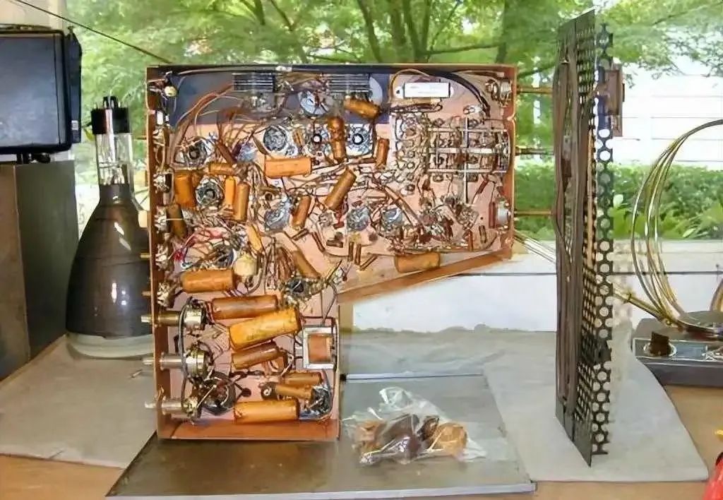
An old Motorola television from 1948, without PCB.
Despite the lack of PCBs, we did see the arrival of the transistor at Bell Labs in 1947. It took another six years before this device was finally used in products, but why so long? In those days, information was disseminated through journals, conferences, etc. Before the information age, the dissemination of information simply took time.
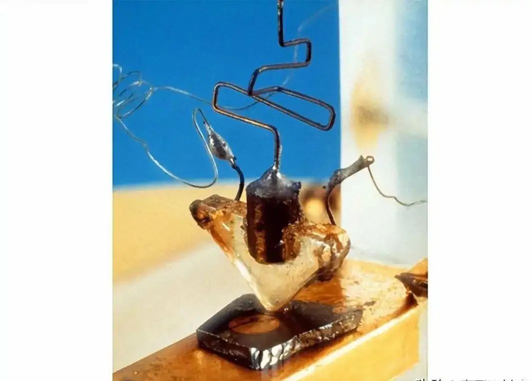
The first transistor, born in 1947 at Bell Labs.
The Cold War Era (1947 – 1991)
The arrival of the Cold War era marked a period of tension between the U.S. and the Soviet Union. Due to the differences between capitalism and communism, these two giants were almost at war with each other, putting the world at risk of nuclear destruction.
To stay ahead in this arms race, both sides had to strengthen their communication capabilities to understand what the enemy was doing. Here, we see PCBs being fully utilized. In 1956, the U.S. Army published a patent for the “Circuit Assembly Process.” Now manufacturers had a method to both secure electronic products and establish connections between components with copper traces.
As PCBs began to take off in manufacturing, we found ourselves participating in the world’s first space race. Russia achieved some amazing feats during this time, including:
-
1957 launch of the first artificial satellite, Sputnik
-
1959 launch of the first spacecraft to the moon, Luna 2
-
1961 sending the first astronaut, Yuri Gagarin, to orbit Earth
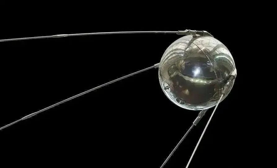
The first artificial satellite, Sputnik, launched by Russia in 1957.
Where was America in all this? Mostly lagging behind, usually taking a year or two to develop the same technology. In response to this gap, we saw the U.S. space budget grow fivefold in 1960. We also had the famous 1962 Kennedy speech, part of which is worth quoting:
“We choose to go to the moon! We choose to go to the moon in this decade and do the other things, not because they are easy, but because they are hard; because that goal will serve to organize and measure the best of our energies and skills; because this challenge is one that we are willing to accept, one we are unwilling to postpone, and one we intend to win.” — U.S. President John F. Kennedy, September 12, 1962
All of this led to a historic milestone. On July 20, 1969, America landed the first man on the moon.
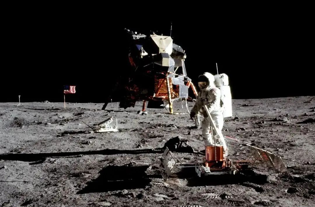
The first man on the moon, a historic moment for humanity.
Back to PCBs, in 1963, we saw Hazeltyne Corporation apply for the first patent for plated through-hole technology. This would allow components to be tightly packed on PCBs without worrying about cross-connections. We also saw the introduction of surface mount technology (SMT) developed by IBM. These dense components were first used in the Saturn rocket boosters.
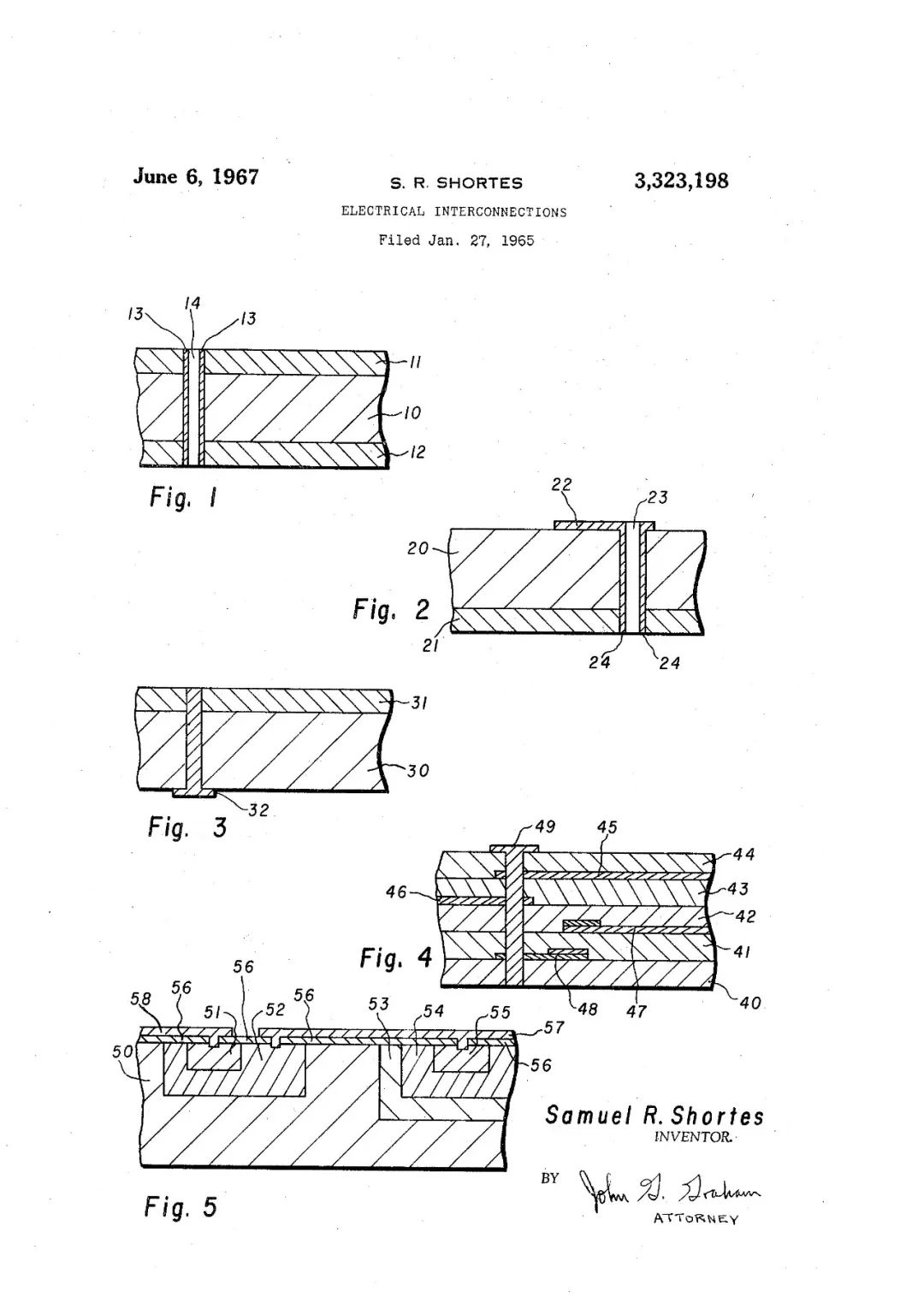
The first through-hole PCB technology patent in 1967.
The Dawn of Microprocessors (1970s)
The 70s brought us the first microprocessors in the form of integrated circuits (ICs). This was initially developed by Jack Kilby of Texas Instruments in 1958. Kilby was a newcomer at TI, so his innovative ideas for ICs were largely kept secret. However, when TI’s senior engineers were sent off to a week-long conference, Kilby stayed behind to run with ideas in his mind. Here, he developed the first IC in the TI lab, and the returning engineers loved it.
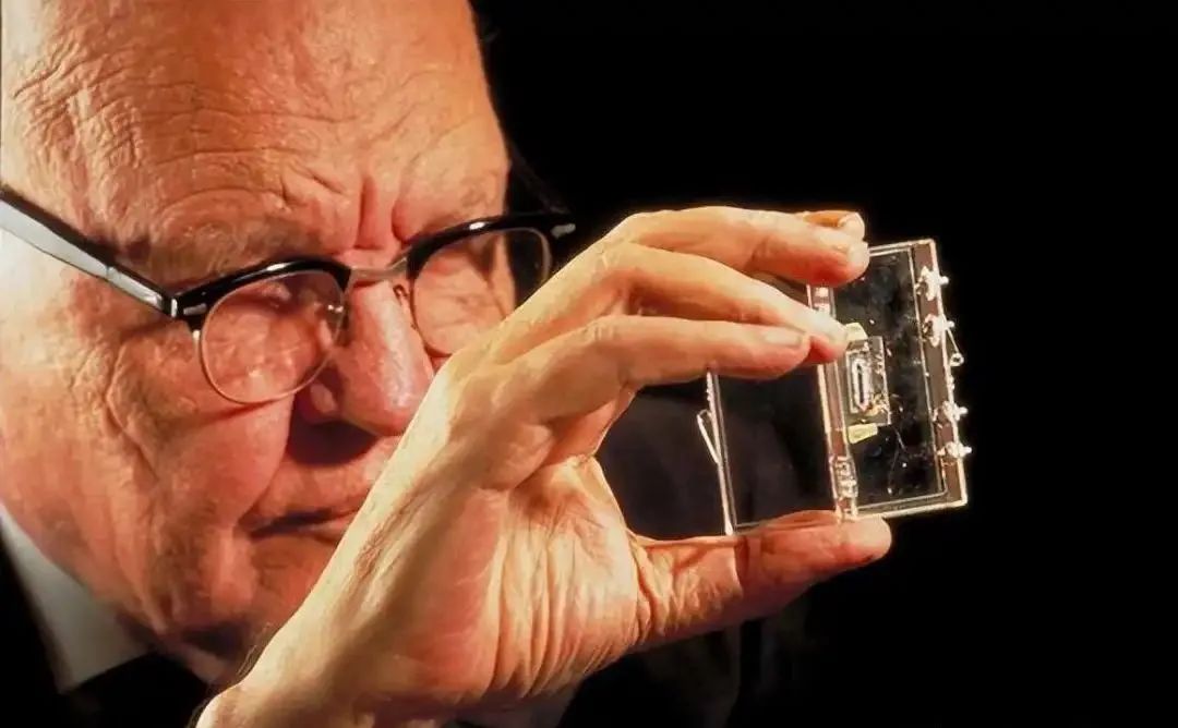
Jack Kilby holding the first integrated circuit.
In the 1970s, we saw ICs used for the first time in electronic product manufacturing. By this time, if you were not using PCBs for connections, you were in big trouble.
The Dawn of the Digital Age (1980s)
The digital age brought about a massive change in how we consume media, introducing personal devices like CDs, VHS, cameras, gaming consoles, and Walkmans.
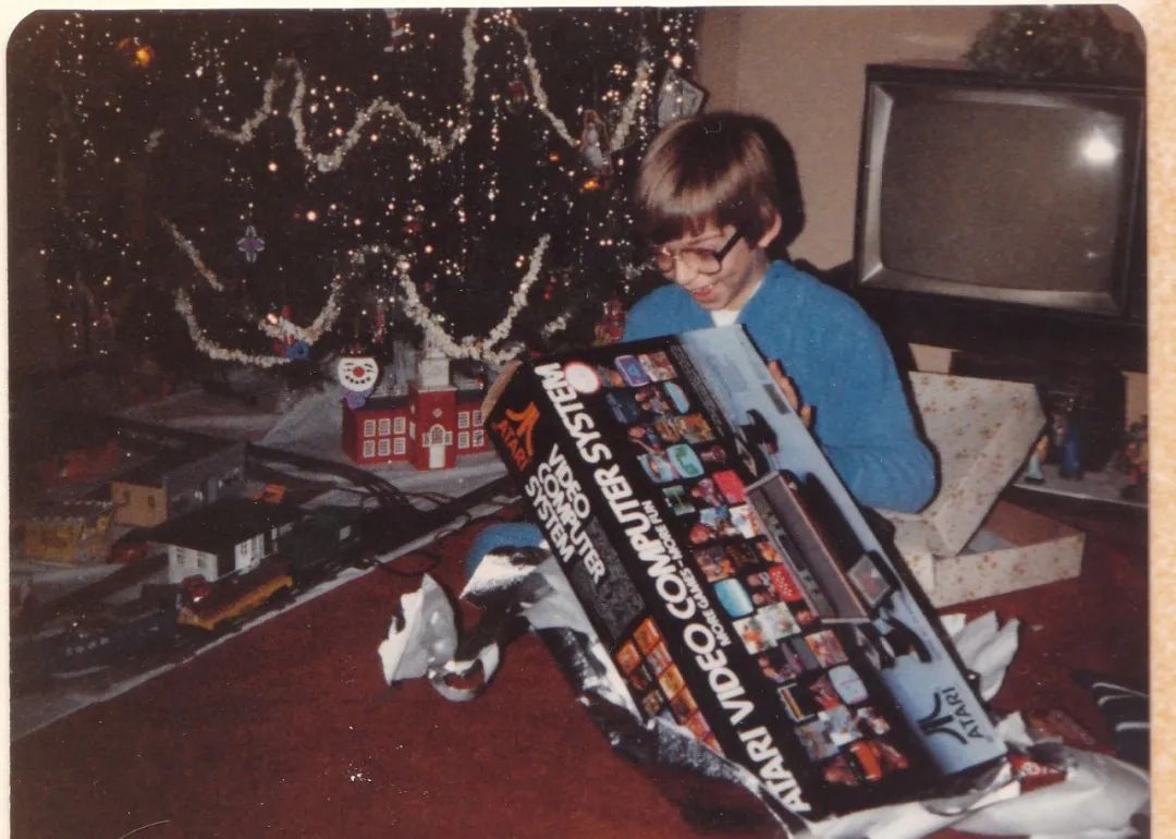
In 1980, the Atari video game console made children’s dreams come true.
It’s important to note that PCBs were still hand-drawn using light boards and templates, but then computers and EDA emerged. Here, we saw EDA software like Protel and EAGLE revolutionizing the way we design and manufacture electronics. Now we could save designs as Gerber text files instead of photos of PCBs, with coordinates that could be input into manufacturing machinery to produce PCBs.
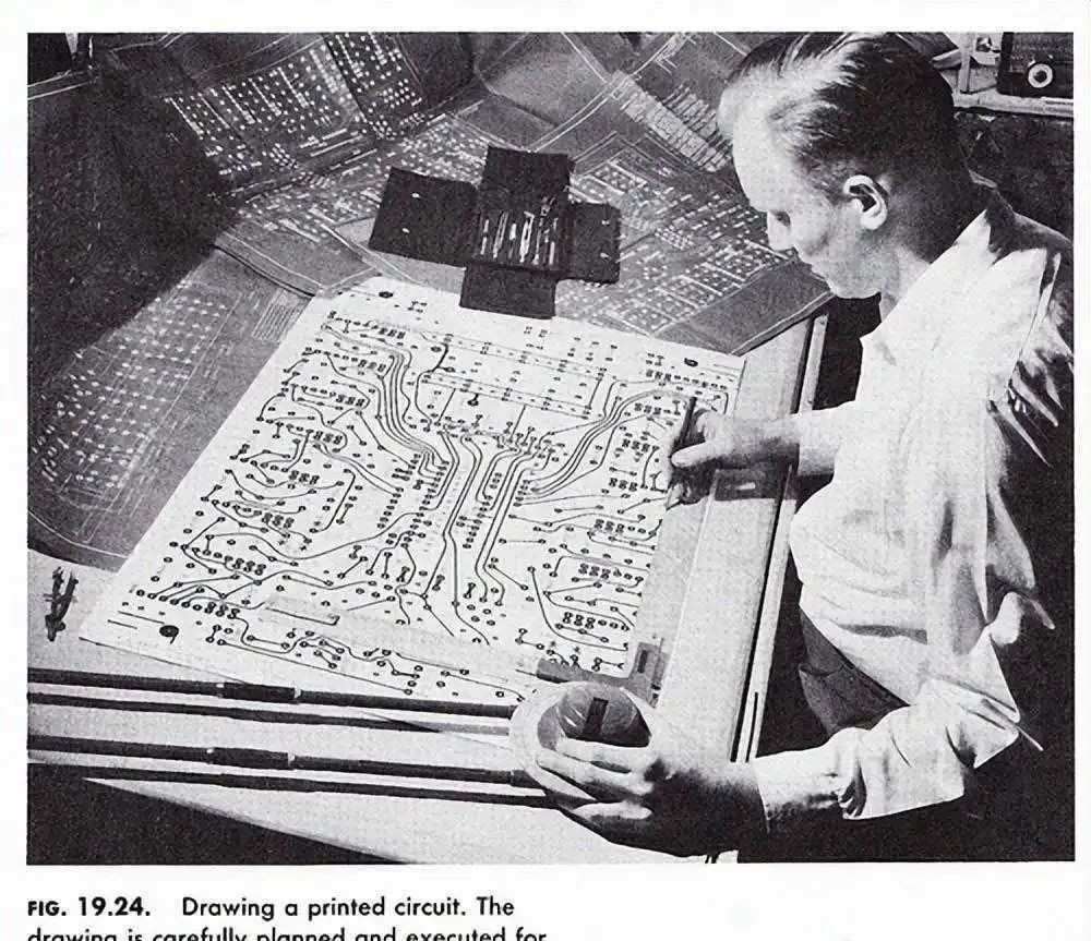
Drawing printed circuit boards with tape and polyester film before EDA arrived.
The Internet Age (1990s)
In the 90s, with the introduction of BGA, we saw the use of silicon fully unfold. Now we could install more gates on a single chip and began embedding memory and system on chip (SoC) together. This was also a time of high miniaturization of electronic products. We did not see any new functions added to PCBs, but the entire design process began to change and evolve, shifting towards ICs.
Now designers had to implement design for test (DFT) strategies in their layouts. It wasn’t easy to pop out a component and add a blue line. Engineers had to design their layouts from the perspective of future rework. Would the way all these components were placed allow for easy removal? This was a huge concern.
This was also an era where smaller component packages like 0402 made hand soldering of circuit boards nearly impossible. Designers now lived in their EDA software, while manufacturers were responsible for physical production and assembly.
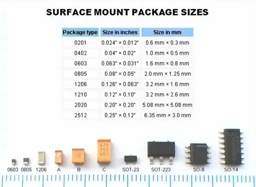
Surface mount components from large to small.
The Hybrid Era (2000s and beyond)
Entering the current era of electronics and PCB design; we call it the hybrid era. In the past, we had multiple devices to meet various needs. You needed a calculator; you bought a calculator. You wanted to play video games; you bought a gaming console. Now you can buy a smartphone and get 30 different built-in functions. This may seem very obvious, but when you really see all the things our smartphones can do, it’s quite shocking:
|
Gaming device |
Address book |
|
Barcode scanner |
|
Flashlight |
Clock |
Camera |
Navigation |
|
Music player |
Schedule |
Video recorder |
Maps |
|
Web browser |
Calendar |
Movie player |
Calculator |
|
Phone |
Notepad |
Tickets |
Recorder |
|
Answering machine |
Text messaging |
Banking |
Books |
We are in a time of device integration, but what will happen next? PCBs have been established, and almost everything we have has processes and procedures. High-speed applications are becoming the norm. We also see that only 25% of PCB designers are under 45, while 75% are preparing for retirement. The industry seems to be in a crisis period.
Will the future of PCB design be robots? Perhaps in wearable devices with flexible circuits? Or we might see protons replace electrons with photonics. As for the physical PCBs we know, even that may change in the future. There may be no need for a physical medium to achieve connections between components, but rather the potential of wave technology. This would allow components to wirelessly send signals without the need for copper.
What does the future hold?
No one really knows the future direction of PCB design, or even the future direction of electronic products. It has been nearly 130 years since our manufacturing muscles began to operate. Since then, with the introduction of major products like automobiles, appliances, computers, smartphones, and more, the world has changed forever. The days of relying on coal, wood, or oil for our basic livelihoods and survival are long gone. Now we have electronic products that meet our daily needs.
But what will the future be? That is a big unknown. It is well known that every invention we face stands on the shoulders of its predecessors. Our ancestors brought PCB design to where it is today, and now we need innovation and a radical change in how we design and interact with technology. The future can be anything. The future depends on you.
This article is adapted from “Artificial Intelligence Science and Technology”
(End)
More exciting:
Yan Shiyi | Reflections and Suggestions on the “Dilemma” of Young University Teachers
【Directory】”Computer Education” 2022 No. 9
【Directory】”Computer Education” 2022 No. 8
【Directory】”Computer Education” 2022 No. 7
【Directory】”Computer Education” 2022 No. 6
【Directory】”Computer Education” 2022 No. 5
【Editorial Message】Professor Li Xiaoming of Peking University: Thoughts on the “Year of Classroom Teaching Improvement”…
Professor Chen Daoxu of Nanjing University: Teaching students to ask questions and teaching students to answer questions, which is more important?
【Yan Shiyi Series】: Trends in Computer Discipline Development and Their Impact on Computer Education
Professor Li Xiaoming of Peking University: From Fun Mathematics to Fun Algorithms to Fun Programming—A Path for Non-specialist Learners to Experience Computational Thinking?
Reflections on Several Issues in Building First-class Computer Disciplines
New Engineering and Big Data Professional Construction
Other stones can attack jade—Compilation of Chinese and Foreign Computer Education Research Articles