Voltage withstanding refers to the maximum voltage that a PCB can withstand under specified conditions without experiencing breakdown. Breakdown occurs when the voltage exceeds a certain limit, causing the insulating material of the PCB to lose its insulating properties, resulting in a sudden increase in current and circuit failure.
Voltage withstand control is a key aspect to ensure the safe and reliable operation of PCBs in high-voltage environments. The following are the core points.
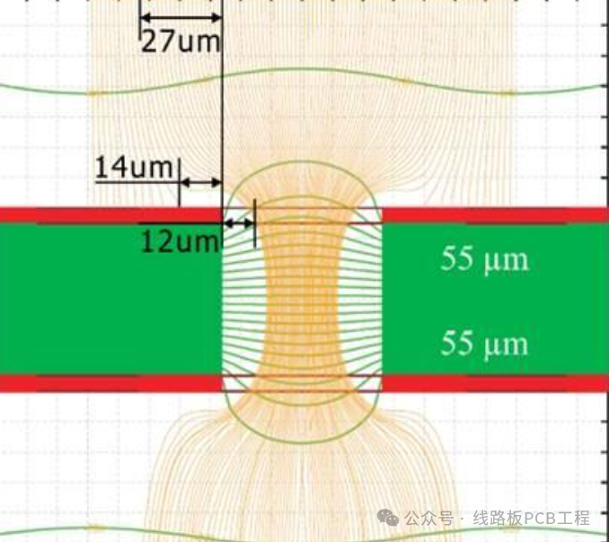
1. Factors Affecting Voltage Withstanding
1. Material Properties
Different materials have different dielectric strengths; the higher the dielectric strength, the greater the electric field intensity the material can withstand, and correspondingly, the better the voltage withstand performance. When selecting materials, high TG FR4 should be prioritized for its better stability.
The typical voltage withstand value for FR4 substrate is 1000V/1mm (approximately 40V/mil), and the voltage withstand of the green solder mask is about 20kV/mm (0.5mil thickness corresponds to 250V).
Dielectric strength is directly related to the type of material (such as FR4) and thickness; increasing the thickness of the interlayer dielectric by 1mil can enhance the voltage withstand capability by approximately 300V-500V.
2. Design Specifications
The spacing between conductors must meet safety distances (to avoid sharp corners), including spacing between lines, spacing between lines and pads, and spacing between pads. The smaller the spacing between conductors, the more concentrated the electric field intensity, making breakdown more likely, thus degrading voltage withstand performance; conversely, increasing the spacing can reduce electric field intensity and improve the voltage withstand performance of the PCB.
During the design process, the spacing between conductors should be reasonably determined based on the working voltage of the PCB. Generally, the higher the working voltage, the larger the required conductor spacing. For example, for a PCB with a working voltage of 220V, the minimum conductor spacing usually needs to exceed 0.5mm; for high-voltage PCBs, the conductor spacing must be strictly calculated and designed based on the specific voltage value.
In lamination design: the voltage withstand stability of inner-layer to inner-layer (core material) is usually better than that of outer-layer to inner-layer (PP layer); the thickness of the interlayer dielectric is significantly related to voltage withstand, for instance: for a voltage withstand of 3600V, the interlayer dielectric should be designed to be≥0.3MM.
3. Process Control
Parameters such as pressing pressure, temperature rise rate, PP voids, and core board cracks can lead to voltage withstand failure; moisture absorption or foreign material residue may reduce insulation performance.
4. Environmental Factors
Environmental factors can also affect the voltage withstand performance of PCBs. High humidity environments can cause the insulating materials of PCBs to absorb moisture, leading to a decrease in dielectric strength and thus reducing voltage withstand performance; excessively high temperatures can accelerate the aging of insulating materials, shortening their lifespan and affecting their voltage withstand performance.
Additionally, dust, corrosive gases, and other contaminants can pollute the surface of PCBs, damaging the insulation layer and reducing voltage withstand performance. Therefore, during the design and use of PCBs, it is necessary to consider the impact of environmental factors and take appropriate protective measures, such as moisture-proof and corrosion-resistant treatments.
2. Testing Standards and Methods
Common testing methods include voltage withstand testing (AC/DC) and insulation resistance testing.
Voltage withstand testing involves applying a certain voltage between different conductors on the PCB and maintaining it for a specified time to observe whether breakdown occurs. The test voltage is usually 1.5-2 times the working voltage, and the test duration is determined according to relevant standards.
Insulation resistance testing measures the insulation resistance value between different conductors on the PCB; the larger the insulation resistance value, the better the insulation performance. Through these two tests, the voltage withstand performance of the PCB can be effectively verified to meet design requirements.
————————————————————
Previous Reviews:
Detailed Explanation of PCB’s CAF Resistance PerformancePCB Warpage Control SolutionsHow to Prevent Breakdown Issues in PCBs