Background
The core algorithm of the product I have been researching these days is the phase difference detection of the sine signals transmitted and received.
On the STM32F407 processor, high-speed sampling of the received and transmitted signals is performed through DMA+SPI communication.
An algorithm is designed to calculate the phase difference between the received and transmitted signals.
A simple debugging upper computer software was modified using Delphi.
The lower computer sends the collected A/D values and calculation results to the upper computer via serial port.
The upper computer displays the data in a graphical interface while performing statistical analysis on the calculation results to determine the correctness of the algorithm,
and adjusts parameters based on the analysis results.
After spending two evenings, I completed the algorithm design, code writing, and debugging for both the upper and lower computers.
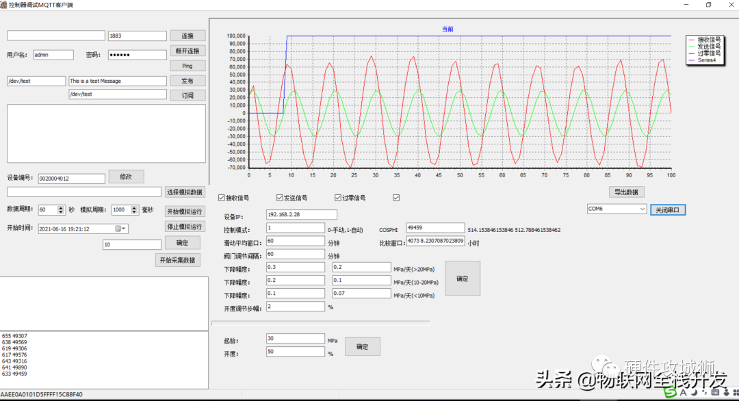
User interface of the upper computer software for product debugging
Circuit Analysis
Tonight I started analyzing the test results.
The first step is to compare it with the theoretical analysis of the hardware circuit.
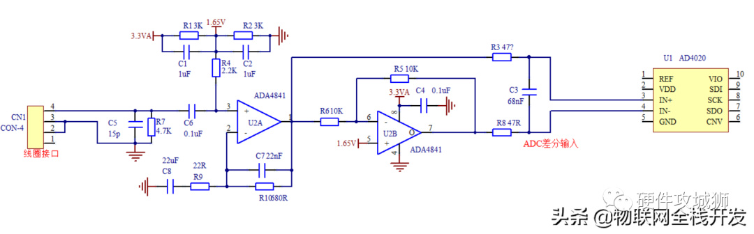
The circuit designed by the customer
The input signal frequency is 4kHz-18kHz.
In this circuit,
The impedance of C1 and C2 is: 
Compared to its series resistor R4, it can be neglected.
Similarly, the impedance of capacitor C8 is  , which can also be neglected compared to R9.
+3.3V is divided through R1 and R3 to obtain 1.65V, providing a DC working level for the rail-to-rail operational amplifier ADA4841, allowing it to be powered by a single supply.
Considering all factors, the AC path of this circuit can be obtained, as shown in the following figure:
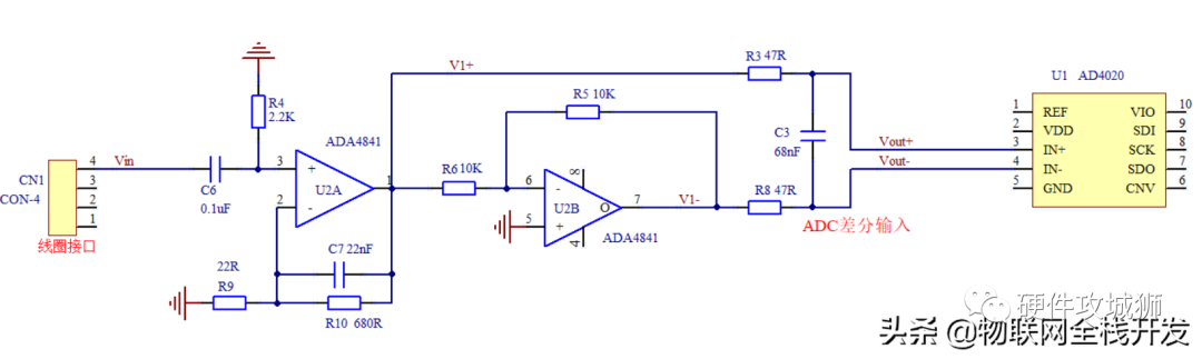
AC path of the circuit
Phase Analysis
Resistor R4 and capacitor C6 form a high-pass filter,
The transfer function is:

The amplitude function is:
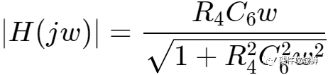
-3dB cutoff frequency is 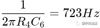
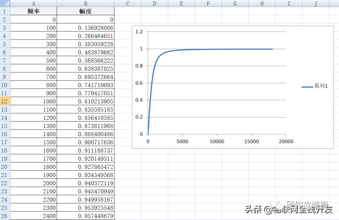
Amplitude-frequency characteristic curve
The phase angle function is:

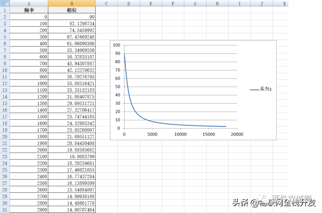
Phase-frequency characteristic
When the frequency is 18KHz, the voltage at the non-inverting input of the operational amplifier leads the input voltage by  ,
,
The amplitude ratio is 1.
R9, R10, and C7 form a low-pass filter, and the transfer function from the operational amplifier’s non-inverting terminal to the output terminal is:

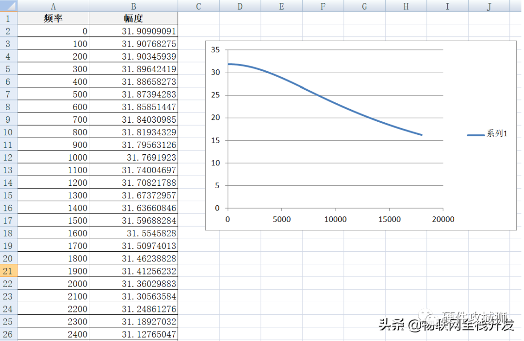
Amplitude-frequency characteristic curve
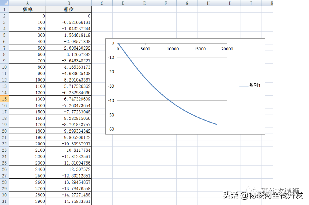
Phase-frequency characteristic curve
When the frequency is 18KHz, the voltage at the output of the operational amplifier lags behind the voltage at the non-inverting input by 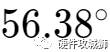 , with an amplitude ratio of 16.25.
Therefore, when the frequency is 18KHz, the output of the operational amplifier lags behind the input signal by 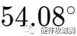 .
.
The differential input signal Vout+-Vout- of the AD4020 and the differential signal V1+-V1- at the output of the operational amplifier in the frequency domain satisfy the following relationship:

When the frequency is 18KHz, the input signal of the AD4020 lags behind the output signal of the operational amplifier by 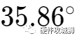 , with an amplitude ratio of 0.81.
In summary, the processing circuit causes a phase lag of 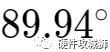 .
.
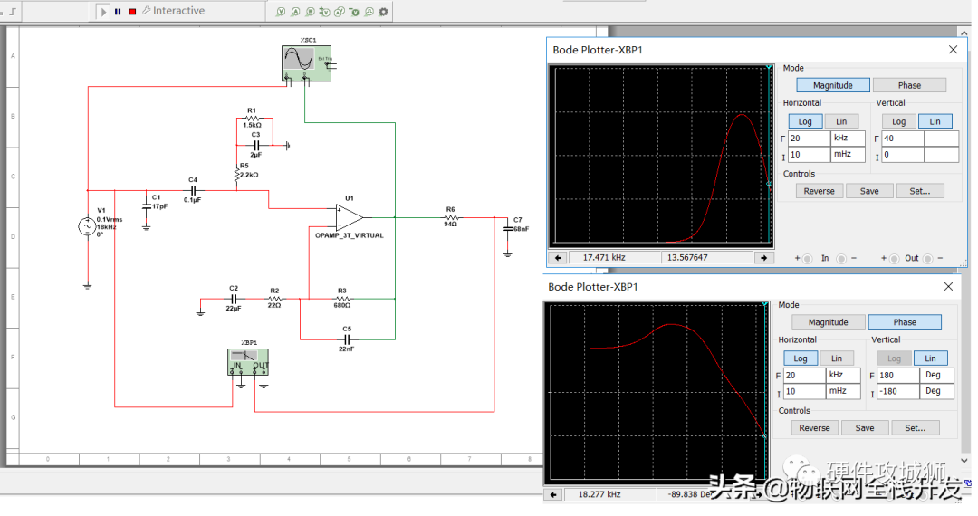
Multisum Simulation
The Multisum simulation is consistent with the calculation results.
Source: Full-Stack Development of IoT
Link: https://www.toutiao.com/article/6992161470188470798
 Statement: This article is reprinted from “Toutiao”, and the copyright belongs to the author. If there is any infringement, please contact us for deletion!❤「If useful, please share」❤
👇Click Follow, Technology to receive timely delivery of dry goods!👇

-
Wonderful Operational Amplifier Circuits
-
This is the book that every electronic engineer must read! Amazing!
-
Why 50 ohms???
-
The most detailed basics of diodes
-
What is a BSP engineer?
-
How to play with the ubiquitous ESP8266?
-
General Principles of PCB Layout and Wiring in AD
-
Voltage Collection Sampling Circuit Design
Please like and share if you enjoy, good articles need your support and encouragement