From WeChat Official Account: Zeiss Industrial Quality Solutions
In the rapidly evolving era of artificial intelligence (AI) technology, its powerful development momentum places higher demands on the quality of PCB (Printed Circuit Boards). As a key component of AI server hardware architecture, the performance and reliability of PCBs directly affect the operational efficiency of AI systems. With the increasing demands for data processing speed and accuracy in AI servers, the application of PCBs is becoming more widespread. However, microstructural issues such as via defects and copper residue have become critical factors hindering improvements in reliability.
Challenges of HDI Board Vias
Although multi-layer high-density interconnect (HDI) boards offer advantages such as high-density wiring, ultra-low loss materials, and thermal management, their complex via processes still pose quality risks.
Manufacturing Process
Blind vias are used in a stacked manner to achieve inter-layer connectivity. For via design, the blind vias in the inner layers must undergo a filling and plating process.
Challenges Encountered
Due to the significant difference in grain size between the base copper and plated copper, connection defects are likely to occur, affecting product reliability.
Solutions
Utilizing FIB technology for precise positioning and analysis, this real-time analysis mode of “cutting while observing” significantly shortens the cycle from defect discovery to mechanism verification, allowing for rapid inspection of via defects.
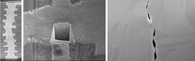
▲ Using FIB technology to locate the ICD defect position at the bottom of the blind via

Copper Residue Detection on SLP Boards
SLP boards are characterized by high density and high integration. SLP requires filling blind vias for subsequent stacking and installation of electronic components, which can lead to poor line uniformity.
Manufacturing Process
MSAP technology is used to fill blind vias under graphic plating.
Challenges Encountered
Excessive copper areas in the circuitry can cause film entrapment, and the dry film between graphics may not be completely removed, resulting in copper residue after etching that can cause short circuits.
Solutions
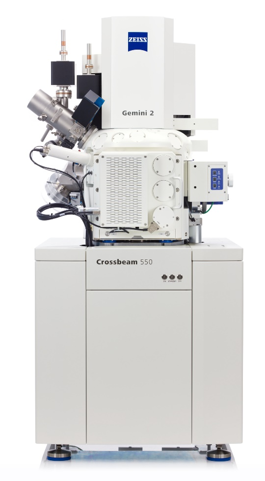
The Zeiss Crossbeam Laser can be used, which integrates femtosecond lasers, gallium ion beams, and field emission scanning electron microscopy (FIB-SEM), combining femtosecond lasers with FIB-SEM to achieve a fast and efficient workflow, accurately locating internal defect positions.
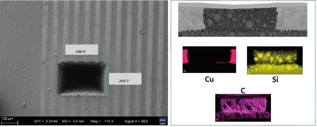
Advantages of the Solution
By processing samples with femtosecond lasers in a vacuum environment, damage and heat-affected zones are effectively avoided, and laser processing is completed in a separate chamber, preventing contamination of the FIB-SEM main chamber and detection.
Zeiss Focused Ion Beam Scanning Electron Microscope Crossbeam FIB Technology Empowers Efficient Analysis
01
High Beam Current Precision
With a beam current control capability of 100nA, it can achieve rapid sample cutting while maintaining high precision, avoiding the over-etching issues of traditional ion beams.
02
High Resolution
High imaging resolution ensures real-time monitoring of microstructural changes during the cutting process, meeting the processing needs of precision scenarios such as PCB micro-holes and FIB clear imaging.
03
Flexible Voltage Control
Ion beam acceleration voltage ranges from 500V to 30kV, reducing sample amorphization damage.
04
Avoiding Magnetic Field Interference Design
Equipped with the ZEISS Gemini electron lens, with a no-leakage design for the objective lens, allowing electron and ion beams to operate simultaneously, achieving better edge cutting.
For more solutions and applications
Welcome to register for the Zeiss Industrial Microscope Electronics Industry
Failure Analysis Seminar
Zeiss Industrial Quality Solutions will hold
March 14
in Songshan Lake, Dongguan
Seminar format: Theory sharing + hands-on demonstration
If interested
Please scan the QR code below to fill in registration information and reserve a seat
Registration deadline: 2025/3/2
We will contact you as soon as possible based on the information provided


☑Product Procurement

☑Technical Support

☑After-Sales Service

This article is owned by Zeiss Industrial Quality. Unauthorized reproduction to other official accounts is prohibited. For reproduction, please contact the staff and indicate the source. If there are copyright issues, please contact us.
 |
 |
 |
 |
 |
 |