When starting a new design, we often spend most of our time on circuit design and component selection, and during the PCB layout and routing phase, we may overlook important considerations due to lack of experience.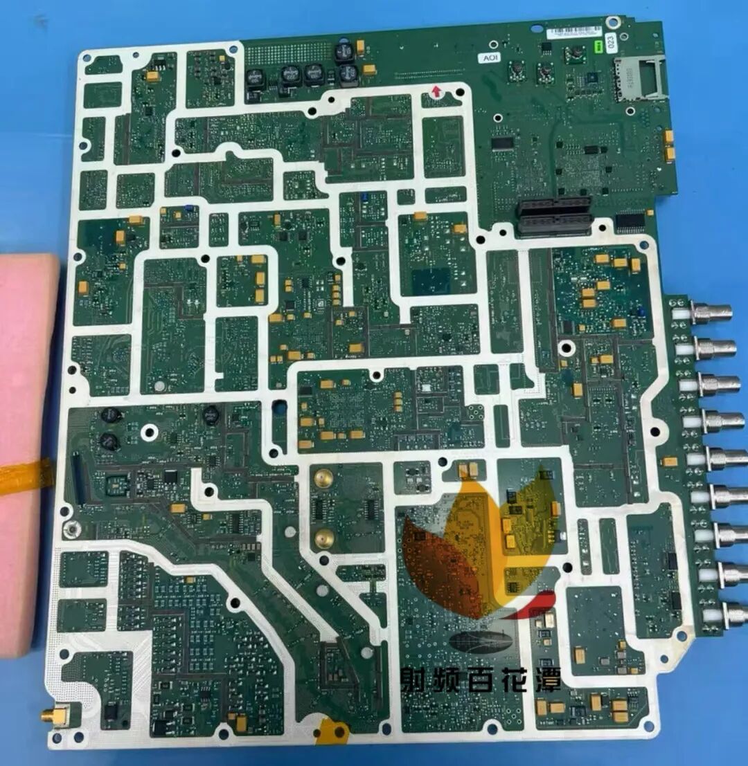 If sufficient time and effort are not allocated to the PCB layout and routing phase, it may lead to issues during the manufacturing stage when the design transitions from the digital realm to physical reality, or result in functional defects.So, what is the key to designing a circuit board that is reliable both on paper and in physical form?
Let’s explore the following 6 PCB design guidelines that are essential for designing a manufacturable and functionally reliable PCB.
1Refine Your Component Placement
The component placement phase of the PCB layout process is both a science and an art, requiring strategic consideration of the main components available on the circuit board. While this process can be challenging, the way you place electronic components will determine the ease of manufacturing your circuit board and how well it meets your original design requirements.While there are common general orders for component placement, such as sequentially placing connectors, mounting devices, power circuits, precision circuits, critical circuits, etc., there are also specific guidelines to keep in mind, including:Orientation – Ensure that similar components are oriented in the same direction, which will help achieve an efficient and error-free soldering process.Layout – Avoid placing smaller components behind larger components, as this may lead to placement issues due to the soldering of the larger components affecting the smaller ones.Organization – It is recommended to place all surface mount (SMT) components on the same side of the circuit board and all through-hole (TH) components on the top of the circuit board to minimize assembly steps.
Another important PCB design guideline to note – is that when using mixed technology components (through-hole and surface mount components), manufacturers may require additional processes to assemble the circuit board, which will increase your overall costs.
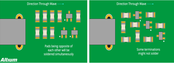
Good chip component orientation (left) and poor chip component orientation (right)
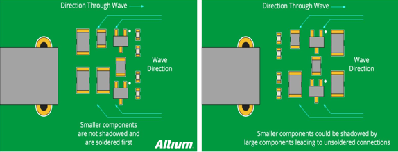
Good component layout (left) and poor component layout (right)
2Proper Placement of Power, Ground, and Signal Traces
After placing the components, the next step is to place power, ground, and signal traces, to ensure that your signals have a clean and fault-free path. During this stage of the layout process, keep the following guidelines in mind:
1) Position Power and Ground Plane Layers
It is always recommended to place power and ground plane layers inside the circuit board while maintaining symmetry and centering. This helps prevent your circuit board from warping, which also relates to whether your components are correctly positioned. For powering ICs, it is advisable to use a common channel for each power line, ensuring a robust and stable trace width, and avoiding daisy-chaining power connections between components.
2) Signal Trace Connections
Next, connect the signal traces according to the design in the schematic. It is recommended to always take the shortest and most direct path between components. If your components need to be fixed in the horizontal direction without deviation, it is advisable to run traces horizontally at the component exit points on the circuit board, and then switch to vertical traces after exiting. This way, during soldering, as the solder migrates, the components will be fixed in the horizontal direction, as shown in the upper part of the figure below. In contrast, the signal trace method in the lower part of the figure may cause component deflection during soldering due to the flow of solder.
Recommended routing method (arrows indicate solder flow direction)
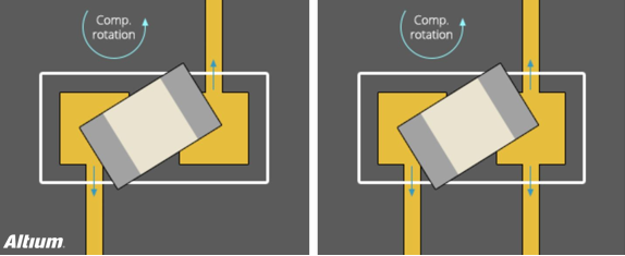
Not recommended routing method (arrows indicate solder flow direction)
3) Define Trace Widths
Your design may require different traces that will carry various currents, which will determine the required trace widths. Considering this basic requirement, it is recommended to provide a width of 0.010’’ (10mil) for low current analog and digital signals. When your trace current exceeds 0.3 Amps, it should be widened. Here is a free trace width calculator to simplify this conversion process.
3Effective Isolation
You may have experienced how large voltage and current spikes in power circuits can interfere with your low voltage control circuits. To minimize such interference issues, follow these guidelines:Isolation – Ensure that each power line maintains separation between power ground and control ground. If you must connect them within the PCB, ensure it is as close to the end of the power path as possible.Layout – If you have placed a ground plane in the middle layer, ensure to place a low impedance path to reduce the risk of interference from any power circuits and help protect your control signals. The same guidelines can be followed to keep your digital and analog signals separate.Coupling – To reduce capacitive coupling due to large ground planes and traces running above and below them, try to cross analog signal lines only through analog ground.
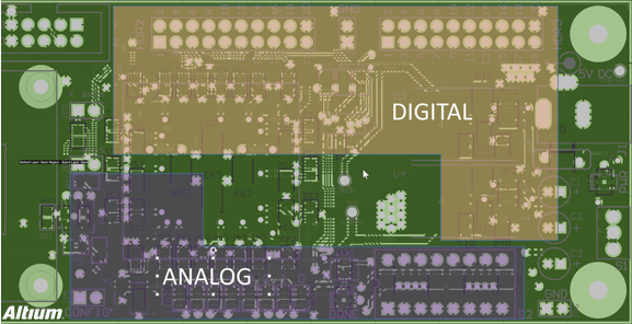
Component isolation example (digital and analog)
4Addressing Heat Issues
Have you ever experienced a decrease in circuit performance or even damage to the circuit board due to heat issues? Many problems arise for designers due to a lack of consideration for heat dissipation. Here are some guidelines to help address heat dissipation issues:
1) Identify Problematic Components
The first step is to consider which components will dissipate the most heat on the circuit board. This can be achieved by first finding the “thermal resistance” rating in the component’s datasheet and then following the recommended guidelines to transfer the generated heat. Of course, heat sinks and cooling fans can be added to keep component temperatures down, and remember to keep critical components away from any high heat sources.
2) Add Thermal Relief Pads
Adding thermal relief pads is very useful for producing manufacturable circuit boards, and they are crucial for high copper content components and wave soldering applications on multilayer circuit boards. Due to the difficulty in maintaining process temperatures, it is always recommended to use thermal relief pads on through-hole components to slow down the heat dissipation rate at the component pins, making the soldering process as simple as possible.As a general rule, always use thermal relief pad connections for any through-holes or vias connected to ground or power planes. In addition to thermal relief pads, you can also add teardrops at the pad connection lines to provide additional copper foil/metal support. This will help reduce mechanical and thermal stress.
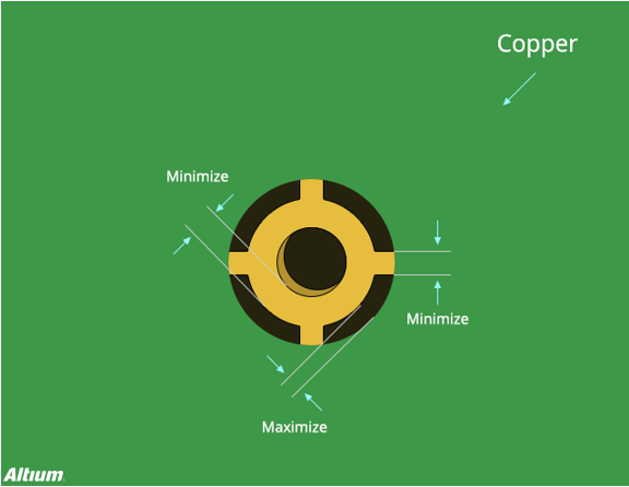
Typical thermal relief pad connection method
5Thermal Relief Pad Basics
Engineers responsible for process or SMT technology in many factories often encounter issues such as solder voids, de-wetting, or cold soldering, regardless of how much the process conditions are changed or how the reflow oven temperature is adjusted, there is still a certain rate of non-wetting. What is the reason for this? Setting aside the issues of component and circuit board oxidation, the root cause is found to be a significant portion of these soldering defects actually stem from deficiencies in the circuit board’s layout design, and the most common issue is that several pins of the component are connected to a large area of copper, causing these component pins to experience soldering defects after reflow soldering. Some hand-soldered components may also encounter similar issues due to the same situation, and some may even be damaged due to excessive heating.
Typically, PCBs often require large areas of copper foil to serve as power (Vcc, Vdd, or Vss) and ground (GND, Ground). These large areas of copper foil are usually directly connected to some control circuits (ICs) and electronic component pins. Unfortunately, when we want to heat these large areas of copper foil to soldering temperatures, it usually takes longer compared to independent pads (meaning heating is slower), and the heat dissipation is also faster. When such large area copper foil traces connect to small resistors or capacitors, it is easy to encounter soldering issues due to inconsistent melting and solidifying times;
If the reflow soldering temperature curve is not well adjusted, and the preheating time is insufficient, the component pins connected to large copper foils are likely to fail to reach soldering temperatures, resulting in cold soldering issues. During hand soldering, these component pins connected to large copper foils may cool too quickly, making it impossible to complete soldering within the specified time.
The most common defects are cold soldering, where the solder only adheres to the component pins and does not connect to the circuit board pads. Visually, the entire solder joint will form a ball shape; furthermore, operators may continuously increase the soldering iron temperature or heat for too long to get the pins soldered to the circuit board, which can cause the components to exceed their heat tolerance and get damaged without them realizing it. As shown in the figure below.
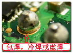
Cold soldering, solder voids, or non-wetting
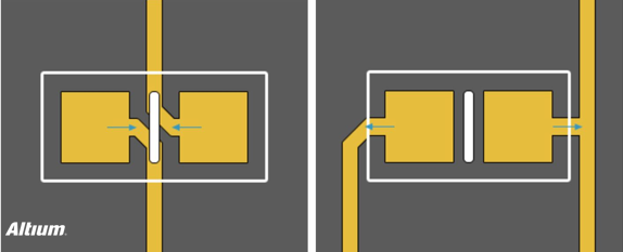
Now that we know the problem points, we can have solutions, we generally require the use of what is called a Thermal Relief pad design to solve these soldering issues caused by connecting component pins to large copper foils.
As shown in the figure below, the left wiring does not use thermal relief pads, while the right wiring has adopted the thermal relief pad connection method, where the contact area between the pad and the large copper foil is reduced to only a few thin lines, significantly limiting the temperature loss at the pad, achieving better soldering results.
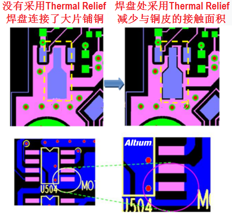
Comparison of Thermal Relief pad usage
6Check Your Work
When you are tirelessly assembling all the parts for manufacturing, it is easy to discover problems only at the end of the design project, feeling overwhelmed. Therefore, double and triple-checking your design work at this stage can mean the difference between successful and failed manufacturing. To assist in completing the quality control process, we always recommend starting with Electrical Rule Check (ERC) and Design Rule Check (DRC) to verify that your design fully meets all rules and constraints. Using these two systems, you can easily check for gap widths, trace widths, common manufacturing settings, high-speed requirements, and short circuits, etc. When your ERC and DRC yield error-free results, it is advisable to check the routing of each signal from the schematic to the PCB, carefully confirming that you have not missed any information by checking one signal line at a time. Additionally, use the detection and shielding features of your design tools to ensure that your PCB layout materials match your schematic.
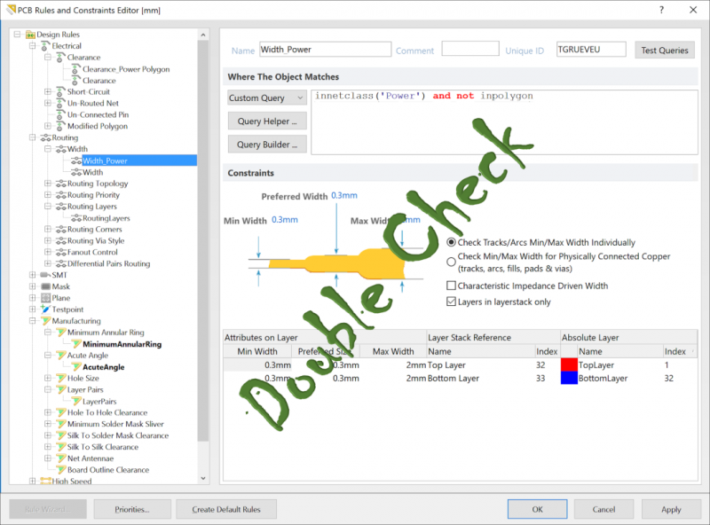
Carefully check your design, PCB, and constraint rules
7Conclusion
By mastering these design guidelines that every PCB designer should know, and by following these recommendations, you will soon be able to design powerful and manufacturable circuit boards with truly high-quality printed circuit boards.
Good PCB design practices are crucial for success, and these design rules lay the foundation for building and reinforcing continuous improvement practices in all design practices.

Disclaimer:
This account maintains neutrality regarding the statements and views of all original and reprinted articles, and the articles are provided for readers’ learning and communication purposes only. The copyright of the articles, images, etc. belongs to the original authors. Some articles have unknown sources; if there is any infringement, please contact for deletion. For submissions/promotions, please add WeChat: 15989459034