In the design and manufacturing process of electronic products, the PCB acts as a bridge connecting various electronic components. Its quality directly affects the overall performance and reliability of the product. Therefore, engineers must conduct strict inspections on the PCB to ensure that the product is flawless and can achieve optimal efficiency and performance. So, what key areas should be inspected?
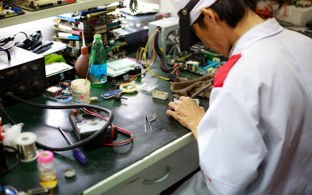
1. Line and Spacing Inspection
Line spacing check: Ensure that the spacing between all lines (including line-to-line, line to component pads, line to through holes, etc.) meets design specifications and production requirements to avoid the risk of short circuits;
Through hole connectivity: Verify that the connections between through holes, lines, and component pads are accurate to ensure circuit conductivity.
2. Power and Ground Design Evaluation
Width and coupling: Assess whether the width of the power and ground wires is sufficient and whether they achieve close coupling to reduce wave impedance and enhance circuit stability;
Optimize space utilization: Check if there is further space on the PCB to widen the ground wire to improve performance.
3. Signal Line Optimization Verification
Key signal line handling: Confirm that effective measures have been taken for key signal lines, such as maintaining the shortest path, adding protection lines, and clearly separating input and output lines to reduce signal interference.
4. Isolation of Analog and Digital Circuits
Independent ground systems: Verify whether the analog circuit and digital ground have their own independent ground systems to reduce mutual interference and enhance overall circuit performance.
5. Graphics and Process Line Inspection
Potential issues with graphics: Confirm that added graphics (such as icons and labels) do not cause signal short circuits, ensuring the safety of the circuit layout;
Process line compliance: Check whether necessary process lines have been added to the PCB and whether the design of the solder mask meets production process requirements, including solder mask dimensions and character positions.
6. Special Considerations for Multi-layer Boards
Power ground layer edge treatment: In multi-layer board design, pay special attention to whether the outer frame edges of the power ground layer are appropriately reduced to prevent copper foil exposure that could lead to short circuit issues.
This article is an original piece by Fan Yi Education. Please indicate the source when reprinting!