When hardware engineers first encounter multi-layer PCBs, it can be quite overwhelming. With layers often reaching ten, the circuits resemble a spider’s web.
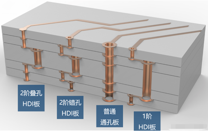
Today, I created several internal structure diagrams of multi-layer PCBs, using 3D graphics to showcase various layered structures within the PCB.
01
The Core of High-Density Interconnection Boards (HDI) Lies in the Via
The processing of multi-layer PCB circuits is not much different from single or double-sided boards; the biggest difference lies in the via technology.
Circuits are etched out, while vias are drilled and then copper-plated, which everyone involved in hardware development understands, so I won’t elaborate further.
Multi-layer circuit boards typically include through-hole boards, first-order boards, second-order boards, and second-order stacked hole boards. Higher-order types such as third-order boards and arbitrary layer interconnection boards are rarely used and are extremely expensive, so I won’t discuss them in detail.
Generally, 8-bit microcontroller products use a 2-layer through-hole board; smart hardware at the 32-bit microcontroller level uses 4 to 6-layer through-hole boards; smart hardware at the Linux and Android levels uses 6-layer through-hole to 8 first-order HDI boards; compact products like smartphones typically use 8-layer first-order to 10-layer second-order circuit boards.
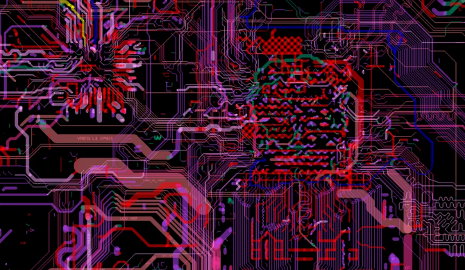
8-layer second-order stacked holes, Qualcomm Snapdragon 624
02
The Most Common Through-Hole
There is only one type of via that runs from the first layer to the last layer. Regardless of whether it is external or internal circuits, the holes are drilled through, known as through-hole boards.
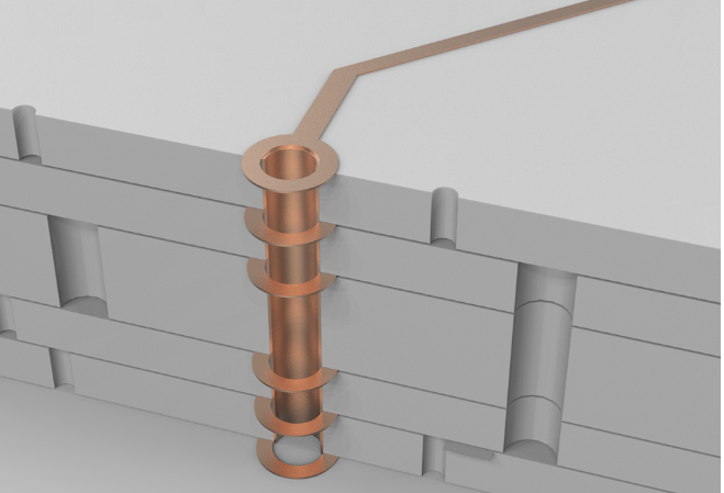
Through-hole boards are not related to the number of layers, as the common 2-layer boards are through-hole boards, while many switches and military circuit boards can have 20 layers and still be through-hole.
Using a drill to penetrate the circuit board, copper is plated in the holes to create a pathway.
It is important to note that the inner diameters of through-holes typically range from 0.2mm, 0.25mm, to 0.3mm, but generally, 0.2mm is significantly more expensive than 0.3mm. This is because thinner drill bits are more prone to breaking and take longer to drill. The additional time and cost of drill bits are reflected in the increased price of the circuit boards.
03
Laser Vias in High-Density Boards (HDI Boards)
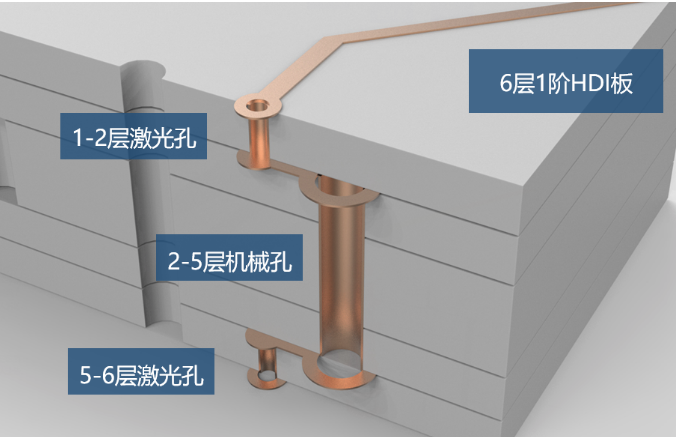
This image shows the layered structure of a 6-layer first-order HDI board, where the top two layers are laser vias with a 0.1mm inner diameter. The inner layers are mechanical vias, equivalent to a 4-layer through-hole board, covered by 2 additional layers.
Lasers can only penetrate glass fiber materials, not metal copper. Therefore, drilling holes on the outer surface does not affect other internal circuits.
After the laser creates the holes, copper is plated to form laser vias.
04
Second-Order HDI Board with Two Layers of Laser Vias
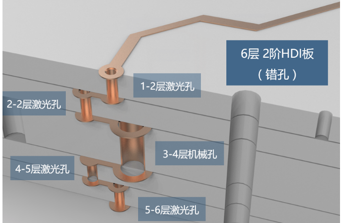
This image depicts a 6-layer second-order staggered hole HDI board. Generally, 6-layer second-order boards are less common, with most starting at 8 layers. The additional layers follow the same principle as the 6-layer.
Second-order refers to having 2 layers of laser vias.
Staggered holes mean that the two layers of laser vias are offset.
Why is it staggered? Because copper plating cannot fill the vias completely, leaving them empty, so you cannot drill another hole directly on top; a certain distance must be maintained before drilling another layer.
6-layer second-order = 4-layer first-order plus 2 layers.
8-layer second-order = 6-layer first-order plus 2 layers.
05
Stacked Hole Boards: Complex Process and Higher Costs
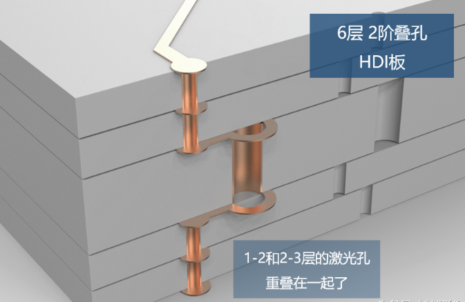
The staggered hole board has two layers of laser vias overlapping. The circuits become more compact.
It is necessary to fill the inner laser vias with electroplating before creating the outer laser vias. This process is more expensive than staggered vias.
06
Extremely Expensive Arbitrary Layer Interconnection Boards with Multi-Layer Laser Stacked Vias
Every layer has laser vias that can connect together. You can route the lines and drill holes however you want.
Layout engineers must feel ecstatic! No more worries about being unable to design!
Procurement teams might cry just thinking about it, as they cost over 10 times more than ordinary through-hole boards!
Thus, only products like the iPhone can afford to use them. I haven’t heard of any other smartphone brands utilizing arbitrary layer interconnection boards.
Conclusion
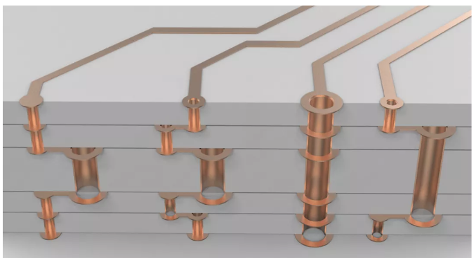
Finally, here’s a picture for a detailed comparison.
Please pay attention to the size of the holes and whether the pads are closed or open.
Disclaimer:This article is copyrighted by the original author and does not represent the association’s views.The articles promoted by the “Jiangxi Province Electronic Circuit Industry Association” are for sharing purposes only and do not represent the stance of this account. If there are any copyright issues, please contact us for removal.