☞ This is the 17006th article published by Metal Processing (mw1950pub).

Editor’s Note
The production of PCB is very complex. Taking a four-layer printed circuit board as an example, the manufacturing process mainly includes PCB layout, core board production, inner layer PCB layout transfer, core board drilling and inspection, lamination, drilling, copper chemical deposition on the hole wall, outer layer PCB layout transfer, and outer layer PCB etching. Today, let’s understand the manufacturing process through animated images.
PCB Manufacturing Process
01
PCB Layout
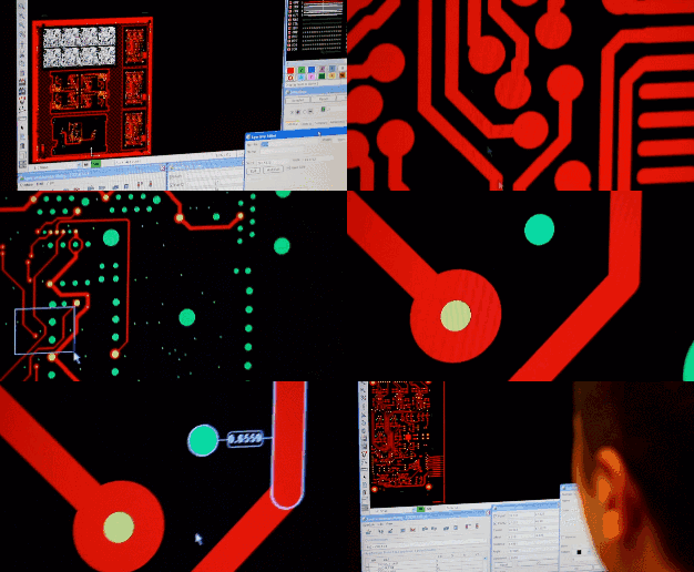
The first step in PCB production is to organize and check the PCB layout. The PCB manufacturing factory receives CAD files from the PCB design company. Since each CAD software has its unique file format, the PCB factory will convert it into a unified format—Extended Gerber RS-274X or Gerber X2. Then, the factory’s engineers will check whether the PCB layout meets the manufacturing process and whether there are any defects.
02
Core Board Production
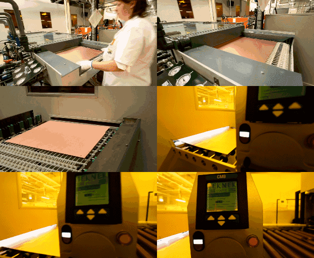
Clean the copper-clad board. Dust can cause short circuits or open circuits in the final circuit.
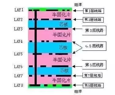
The following image is a diagram of an 8-layer PCB, which is actually made up of 3 copper-clad boards (core boards) plus 2 copper films, then bonded together with prepreg. The production sequence starts from the innermost core board (layers 4 and 5) and continues to stack together, then fixed. The production of a 4-layer PCB is similar, but it only uses 1 core board and 2 copper films.
03
Inner Layer PCB Layout Transfer
First, the two layers of the innermost core board (Core) need to be created. After cleaning the copper-clad board, a layer of photosensitive film is applied to the surface. This film solidifies when exposed to light, forming a protective layer on the copper foil of the copper-clad board.
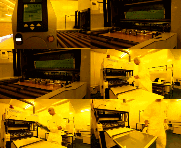
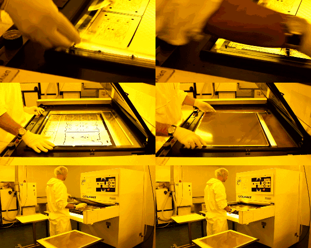
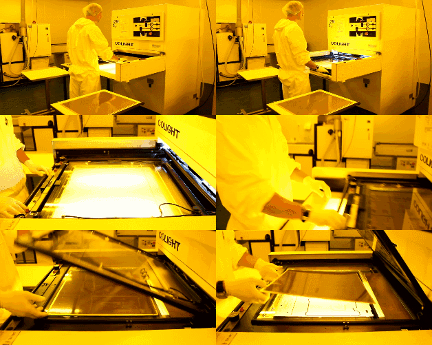
Two layers of PCB layout film and double-sided copper-clad board are then inserted into the upper layer of PCB layout film to ensure the precise alignment of the upper and lower layers of PCB layout films.
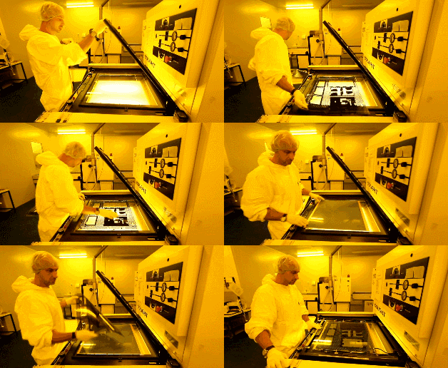
The UV light of the exposure machine irradiates the photosensitive film on the copper foil. Under the transparent film, the photosensitive film is solidified, while the film under the opaque film remains unsolidified. The copper foil covered by the solidified photosensitive film corresponds to the required PCB layout lines, acting similarly to the ink of a laser printer for manual PCBs.
Then, an alkaline solution is used to wash away the unsolidified photosensitive film, leaving the required copper foil lines covered by the solidified photosensitive film.
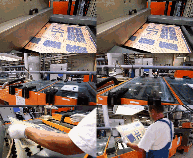
Next, use a strong alkali, such as NaOH, to etch away the unnecessary copper foil.
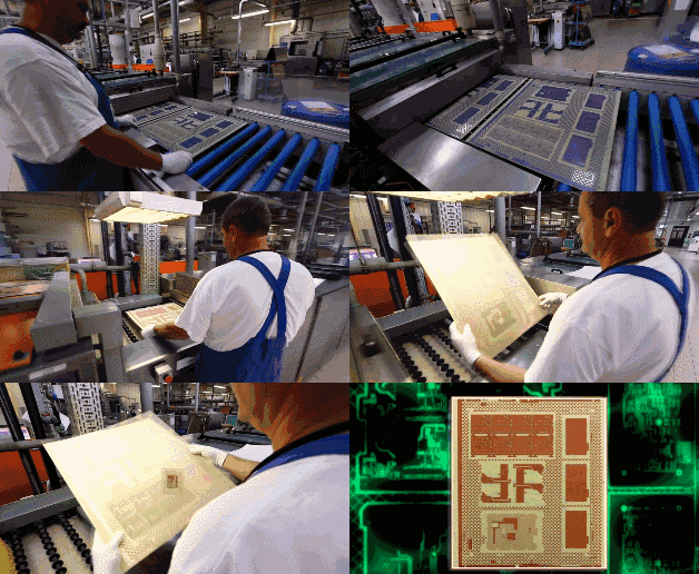
Peel off the solidified photosensitive film to reveal the required PCB layout lines of copper foil.
04
Core Board Drilling and Inspection
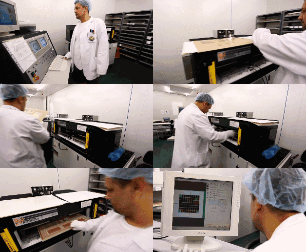
The core board has been successfully produced. Next, alignment holes are drilled in the core board for easy alignment with other materials.
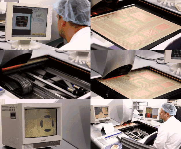
Once the core board is pressed with other layers of PCB, it cannot be modified, so inspection is very important. Machines will automatically compare with the PCB layout drawings to check for errors.
05
Lamination
This step requires a new material called prepreg, which acts as an adhesive between core boards (for PCBs with more than 4 layers) and between core boards and outer copper foils, while also serving as an insulator.
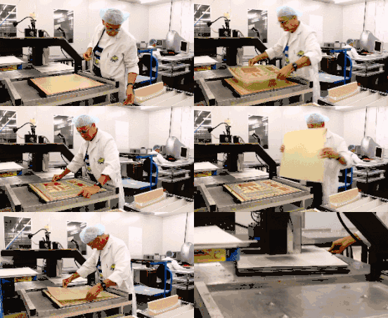
The lower copper foil and two layers of prepreg have been fixed in position through alignment holes and the lower iron plate, then the prepared core board is placed into the alignment holes, and finally, the two layers of prepreg, one layer of copper foil, and one layer of pressure-bearing aluminum plate are covered onto the core board.
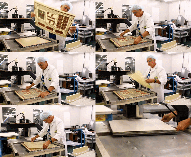
The PCB boards held by the iron plate are placed on a rack and sent into a vacuum hot press for lamination. The high temperature in the vacuum hot press can melt the epoxy resin in the prepreg, fixing the core boards and copper foils together under pressure.
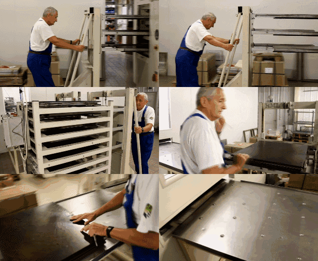 After lamination is completed, remove the upper iron plate that pressed the PCB. Then take away the pressure-bearing aluminum plate, which also isolates different PCBs and ensures the smoothness of the outer copper foil of the PCB. At this point, the PCB taken out will be covered on both sides with a layer of smooth copper foil.
06
Drilling
To connect the four layers of copper foil inside the PCB without contact, first, through-holes must be drilled to penetrate the PCB, and then the hole walls are metallized to conduct electricity.
Use an X-ray drilling machine to locate the inner layer core board. The machine will automatically find and locate the hole positions on the core board, then drill positioning holes in the PCB, ensuring that the drilling will pass through the center of the hole.
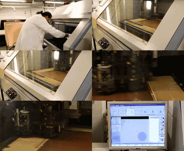
Place a layer of aluminum plate on the drilling machine bed, then place the PCB on top. To improve efficiency, 1 to 3 identical PCB boards can be stacked together for drilling based on the number of layers of the PCB. Finally, cover the top PCB with a layer of aluminum plate. The upper and lower aluminum plates are used to prevent tearing of the copper foil on the PCB when the drill bit enters and exits.
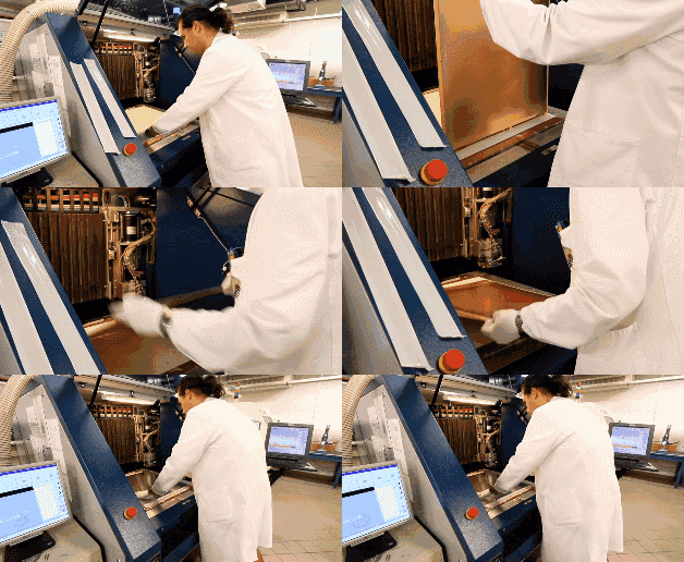
During the previous lamination process, the melted epoxy resin was squeezed out of the PCB, so it needs to be trimmed. The milling machine cuts the perimeter according to the correct XY coordinates of the PCB.
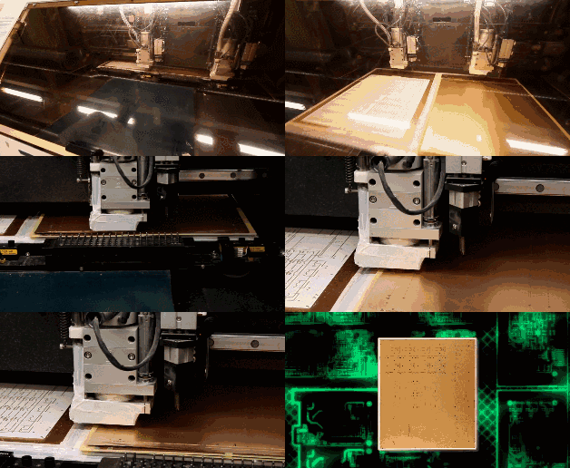
07
Copper Chemical Deposition on Hole Walls
Since almost all PCB designs use through holes to connect different layers of lines, a good connection requires a 25-micron copper film on the hole walls. This thickness of copper film needs to be achieved through electroplating, but the hole walls are made of non-conductive epoxy resin and fiberglass.
So the first step is to accumulate a layer of conductive material on the hole walls, forming a 1-micron copper film on the entire surface of the PCB, including the hole walls, through chemical deposition. The entire process, including chemical treatments and cleaning, is controlled by machines.
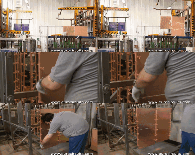
Fix the PCB
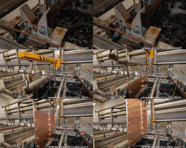
Clean the PCB
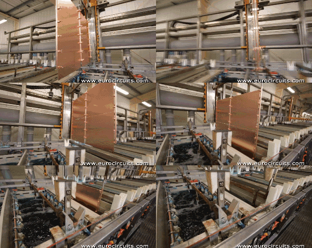
Transport the PCB
08
Outer Layer PCB Layout Transfer
Next, the outer layer PCB layout will be transferred to the copper foil. The process is similar to the previous inner layer core board PCB layout transfer, utilizing photocopying film and photosensitive film to transfer the PCB layout to the copper foil. The only difference is that positive film will be used for the board.
The inner layer PCB layout transfer uses a subtractive method with negative film. The lines on the PCB are covered by the solidified photosensitive film, and the unexposed photosensitive film is washed away. The exposed copper foil is etched, leaving the PCB layout lines protected by the solidified photosensitive film.
The outer layer PCB layout transfer uses a normal method with positive film. The solidified photosensitive film covers the non-line areas on the PCB. After washing away the unexposed photosensitive film, electroplating is conducted. Where there is film, electroplating is not possible, while in areas without film, copper is plated first, followed by tin. After stripping the film, alkaline etching is performed, and finally, the tin is stripped. The line patterns remain on the board due to the protection of the tin.
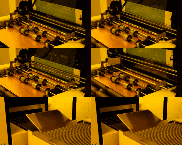
Clamp the PCB with clips and proceed with copper electroplating. As mentioned earlier, to ensure good conductivity at the hole positions, the copper film plated on the hole walls must have a thickness of 25 microns. Therefore, the entire system will be automatically controlled by a computer to ensure precision.
09
Outer Layer PCB Etching
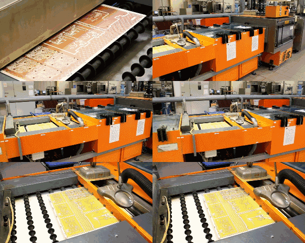
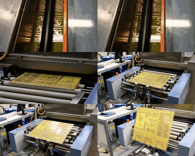
Next, a complete automated production line will complete the etching process. First, the solidified photosensitive film on the PCB board is washed away. Then, strong alkali is used to clean away the unnecessary copper foil covered by it. Finally, the tin plating on the PCB layout copper foil is stripped. After cleaning, the 4-layer PCB layout is completed.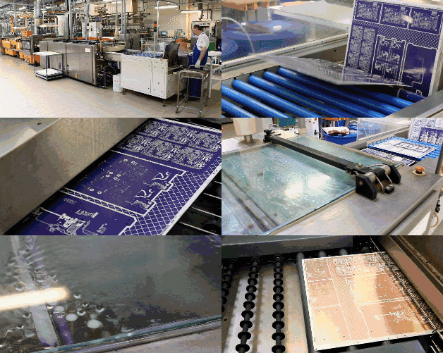
Recommended Video Follow the Metal Processing video account for industrial media with attitude
-End-
☞ Source: EUROCIRCUITS, Mechanical Master ☞ Editor: Shao Yujie ☞ Reviewer: Wu Xiaolan ☞ Media Cooperation: 010-88379790-801 ☞ The only submission website for Metal Processing magazine:http://tougao.mw1950.cn/
Statement: If there are any copyright issues with the videos, images, or text used in this article, please inform us immediately, and we will confirm the copyright based on the proof materials you provide and pay remuneration according to national standards or delete the content immediately!
Statement: If there are any copyright issues with the videos, images, or text used in this article, please inform us immediately, and we will confirm the copyright based on the proof materials you provide and pay remuneration according to national standards or delete the content immediately!