Solder Mask: solder mask refers to the part of the board that is to be coated with green oil; because it is a negative output, the part that actually has the solder mask does not get green oil but is instead coated with tin, appearing silver-white!Paste Mask: paste mask is used during machine placement and corresponds to the pads of all surface-mounted components. Its size is the same as the toplayer/bottomlayer layers and is used for opening the stencil for solder paste application.
Key Points:
Both layers are for soldering and do not refer to one layer for solder and one for green oil. So is there a layer that indicates the area where green oil is applied? As long as there is that layer in a certain area, it indicates that the area is coated with insulating green oil? So far, I have not encountered such a layer! In the PCB we design, the pads on top by default have a solder layer, so the pads on the finished PCB are coated with silver-white solder, and it is not surprising that they are not coated with green oil. However, the routing part of the PCB we design only has the toplayer or bottomlayer, and there is no solder layer, but the routing part on the finished PCB is coated with a layer of green oil.
So it can be understood this way:
1. The solder mask layer means to open windows on the entire solder mask green oil to allow soldering!2. By default, areas without a solder mask layer are to be coated with green oil!3. The paste mask layer is used for surface-mount packaging.SMT packaging uses the toplayer, topsolder, and toppaste layers, where the toplayer and toppaste are the same size, and topsolder is larger by one circle.DIP packaging only uses topsolder and multilayer (after decomposition, it can be found that the multilayer is actually the size overlap of toplayer, bottomlayer, topsolder, and bottomsolder), and topsolder/bottomlayer is larger by one circle than toplayer/bottomlayer.
Question: “The statement ‘The copper layer corresponding to the solder layer must have copper to be plated with tin or gold’ is correct?”
This statement was made by someone working in a PCB factory. His point is that to achieve the effect of plating tin on the part drawn on the solder layer, the corresponding solder layer part must have copper (i.e., the area corresponding to the solder layer must have parts of the toplayer or bottomlayer)! Now we conclude that the statement “The copper layer corresponding to the solder layer must have copper to be plated with tin or gold” is correct; the solder layer indicates the area that does not cover green oil.
-
Mechanical Layer
-
Keepout Layer
-
Top Overlay
-
Bottom Overlay
-
Top Paste
-
Bottom Paste
-
Top Solder
-
Bottom Solder
-
Drill Guide
-
Drill Drawing
-
Multilayer
Mechanical Layer defines the overall appearance of the PCB; when we talk about the mechanical layer, we refer to the entire PCB’s shape and structure.Keepout Layer defines the boundaries for placing components and routing on the PCB. After defining the keepout layer, the electrical lines we route in the future cannot exceed the boundaries of the keepout layer.Top Overlay and Bottom Overlay define the silkscreen characters on the top and bottom layers, which are generally the component numbers and some characters we see on the PCB.Top Paste and Bottom Paste refer to the top and bottom pad layers, which indicate the exposed copper pads (for example, if we draw a wire in the top layer routing layer, what we see on the PCB is just a wire covered by green oil, but where we draw a square or a dot on the toppaste layer at the position of this wire, the square and dot on the produced board will not have green oil but will be copper foil.Top Solder and Bottom Solder are the opposite of the previous two layers; these two layers are meant to be covered by green oil. Since it is a negative output, the part that actually has the solder mask does not get green oil but is plated with tin, appearing silver-white!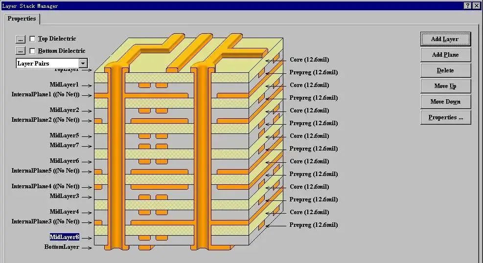 1. Signal Layer is mainly used to lay out the wires on the PCB. Protel 99 SE provides 32 signal layers, including Top Layer, Bottom Layer, and 30 MidLayers.2. Internal Plane Layer Protel 99 SE provides 16 internal power/ground layers. This type of layer is used only for multilayer boards, mainly for laying out power and ground lines. We refer to double-sided boards, four-layer boards, six-layer boards, generally indicating the number of signal layers and internal power/ground layers.3. Mechanical Layer Protel 99 SE provides 16 mechanical layers, which are generally used to set the outer dimensions, data markings, alignment marks, assembly instructions, and other mechanical information of the circuit board. This information may vary according to the requirements of design companies or PCB manufacturers. Executing the menu command Design|Mechanical Layer can set more mechanical layers for the circuit board. Additionally, the mechanical layer can be attached to other layers for output display.4. Solder Mask Layer applies a coating, such as anti-solder paint, to areas outside the pads to prevent soldering on those areas. The solder mask layer is automatically generated to match the pads during the design process. Protel 99 SE provides two solder mask layers: Top Solder and Bottom Solder.5. Paste Mask Layer (SMD Paste Layer) has a similar function to the solder mask layer, except it corresponds to the pads of surface-mounted components during machine soldering. Protel 99 SE provides two paste mask layers: Top Paste and Bottom Paste. It mainly targets SMD components on the PCB. If the board is entirely populated with DIP (through-hole) components, this layer does not need to output Gerber files. Before placing SMD components on the PCB, solder paste must be applied to each SMD pad, and the stencil used for applying solder paste must require this Paste Mask file to be processed. One important point to clarify about the Gerber output of the Paste Mask layer is that this layer mainly targets SMD components, and it is essential to compare this layer with the previously mentioned Solder Mask to understand their different functions.6. Keep Out Layer defines the effective areas for placing components and routing on the PCB. A closed area is drawn on this layer as the effective routing area, and automatic layout and routing cannot occur outside this area.7. Silkscreen Layer is mainly used for placing printed information, such as component outlines and labels, various annotation characters, etc. Protel 99 SE provides two silkscreen layers: Top Overlay and Bottom Overlay. Generally, various annotation characters are on the top silkscreen layer, while the bottom silkscreen layer can be closed.8. Multi Layer pads and through-hole vias on the PCB must penetrate the entire PCB, establishing electrical connections with different conductive pattern layers; therefore, the system specifically sets up an abstract layer—multilayer. Generally, pads and vias should be set on the multilayer; if this layer is closed, pads and vias cannot be displayed.9. Drill Layer provides drilling information during the PCB manufacturing process (for example, pads and vias require drilling). Protel 99 SE provides two drill layers: Drill Guide and Drill Drawing.Source: EDN Electronic Technology Design, copyright belongs to the original author. The purpose of reprinting is to share more information and does not represent the position of this account. If there are copyright issues, please contact the backend, and we will handle it as soon as possible.PCB Network City PCB enthusiasts are paying attention
 If you like it, please give me a star