Welcome FPGA engineers to join the official WeChat technical group.
Clickthe blue textto follow us at FPGA Home – the largest and best FPGA engineer community in China.

1. Basic Constraint Methods
To ensure a successful design, all path timing requirements must be accessible to the execution tools. The three most common paths are:
-
Input path (Input Path), using input constraints
-
Register-to-register path (Register-to-Register Path), using cycle constraints
-
Output path (Output Path), using output constraints
-
Specific exception paths (Path specific exceptions), using false paths and multi-cycle path constraints
1.1. Input Constraint
OFFSET IN constraint limits the relationship between input data and the input clock edge.
1.1.1. System Synchronous Input
In a system synchronous interface, the same system clock transmits and receives data. Considering board path delays and clock jitter, the operating frequency of the interface cannot be too high.
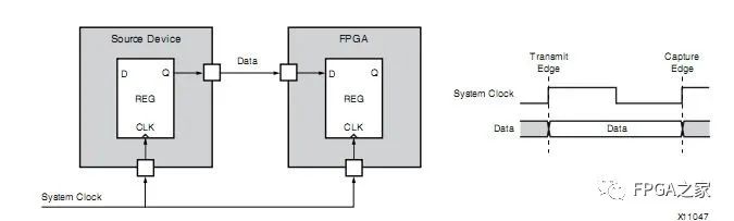
1-1 Simplified system synchronous input SDR circuit diagram
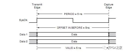
1-2 SDR system synchronous input timing
The above timing constraints can be written as:
NET “SysClk” TNM_NET = “SysClk”;
TIMESPEC “TS_SysClk” = PERIOD “SysClk” 5 ns HIGH 50%;
OFFSET = IN 5 ns VALID 5 ns BEFORE “SysClk”;
1.1.2. Source Synchronous Input
In a source synchronous interface, the clock is generated and transmitted along with the data from the source device.
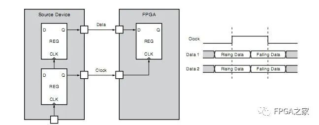
1-3 Simplified source synchronous input DDR circuit
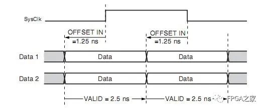
1-4 DDR source synchronous input timing
The timing constraints in the above figure can be written as:
NET “SysClk” TNM_NET = “SysClk”;
TIMESPEC “TS_SysClk” = PERIOD “SysClk” 5 ns HIGH 50%;
OFFSET = IN 1.25 ns VALID 2.5 ns BEFORE “SysClk” RISING;
OFFSET = IN 1.25 ns VALID 2.5 ns BEFORE “SysClk” FALLING;
1.2. Register-to-Register Constraint
Register-to-register constraints often refer to cycle constraints, which cover:
-
Covering the timing requirements of the clock domain
-
Covering the transmission of synchronous data between internal registers
-
Analyzing paths within a single clock domain
-
Analyzing all paths between related clock domains
-
Considering all frequency, phase, and uncertainty differences between different clock domains
1.2.1. Using Clock Devices such as DLL, DCM, PLL, and MMCM to Automatically Determine Synchronization Relationships
Using this type of clock IP Core, you only need to specify their input clock constraints, and the device will automatically constrain the related outputs based on the parameters specified by the user when generating the IP Core, without manual intervention.
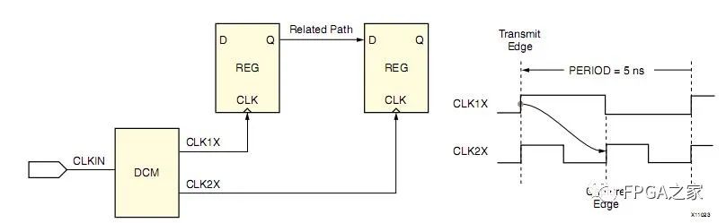
1-5 Clock constraints input to DCM
The timing constraints in the above figure can be written as:
NET “ClkIn” TNM_NET = “ClkIn”;
TIMESPEC “TS_ClkIn” = PERIOD “ClkIn” 5 ns HIGH 50%;
1.2.2. Manually Constrain Related Clock Domains
In some cases, the tool cannot automatically determine the clock timing relationships between synchronized clock domains, and manual constraints are needed. For example, if two clocks with a phase relationship enter the FPGA device from different pins, manual constraints are required for these two clocks.
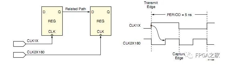
1-6 Related clocks entering the FPGA through two different external pins
The timing constraints in the above figure can be written as:
NET “Clk1X” TNM_NET = “Clk1X”;
NET “Clk2X180” TNM_NET = “Clk2X180”;
TIMESPEC “TS_Clk1X” = PERIOD “Clk1X” 7.5 ns;
TIMESPEC “TS_Clk2X180” = PERIOD “Clk2X180” TS_Clk1X/2PHAS2 + 1.25 ns;
1.2.3. Asynchronous Clock Domains
In asynchronous clock domains, the sending and receiving clocks do not depend on frequency or phase relationships. Since the clocks are unrelated, it is impossible to determine setup time, hold time, and the final relationship of the clock. For this reason, Xilinx recommends using appropriate asynchronous design techniques to ensure successful data acquisition. The Xilinx constraint system allows designers to constrain the maximum delay of data paths without considering the source and destination clock frequencies and phases.
The process for constraining methods used in asynchronous clock domains is:
-
Define timing groups for source registers
-
Define timing groups for destination registers
-
Use From-to and DATAPATHDELAY keywords to define the maximum delay between register groups
1.3. Output Constraint
The output timing constraints restrict the data from internal synchronous components or registers to the device pins.
1.3.1. System Synchronous Output Constraint
The simplified model of system synchronous output is shown in the figure. In the system synchronous output interface, data transmission and acquisition are based on the same clock.
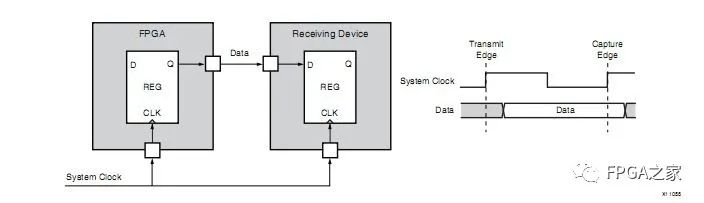
1-7 System synchronous output
The timing constraints can be written as:
NET “ClkIn” TNM_NET = “ClkIn”;
OFFSET = OUT 5 ns AFTER “ClkIn”;
1.3.2. Source Synchronous Output Constraint
In a source synchronous output interface, the clock is regenerated and transmitted along with the data driven by a certain FPGA clock to downstream devices.
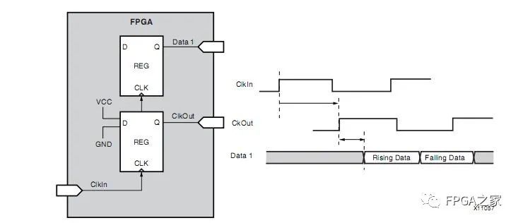
1-8 Simplified circuit timing diagram for source synchronous output
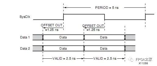
1-9 Timing diagram for a small example of source synchronous output
The timing constraints for the small example can be written as:
NET “ClkIn” TNM_NET = “ClkIn”;
OFFSET = OUT AFTER “ClkIn” REFERENCE_PIN “ClkOut” RISING;
OFFSET = OUT AFTER “ClkIn” REFERENCE_PIN “ClkOut” FALLING;
1.3.3. False Path Constraint
Let SRC_GRP be a group of source registers and DST_GRP be a group of destination registers. If you determine that the paths from SRC_GRP to DST_GRP will not affect timing performance, you can constrain this group of paths as false paths. The tool will skip timing analysis of this group of paths during timing analysis. Such paths are most common in data transmission between registers in different clock domains, as shown in the figure below:
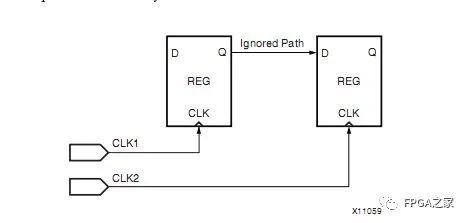
1-10 False path
The constraints can be written as:
NET “CLK1” TNM_NET = FFS “GRP_1”;
NET “CLK2” TNM_NET = FFS “GRP_2”;
TIMESPEC TS_Example = FROM “GRP_1” TO “GRP_2” TIG;
1.3.4. Multi-Cycle Path Constraint
In multi-cycle paths, let the period of the driving clock be PERIOD, and the data can be transmitted from the source synchronous component to the destination synchronous component for a maximum of n*PERIOD time. This constraint reduces the routing difficulty for the tool without affecting timing performance. This constraint is typically used in synchronous component paths controlled by clock enables.
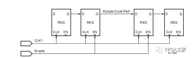
Figure 1-11 Synchronous component path controlled by clock enable
It must be noted that the period for generating the Enable signal in the above figure must be greater than or equal to n*PERIOD, and each Enable transmits one data. Assuming n=2 in the above figure, and MC_GRP is the multi-cycle synchronous component group controlled by clock enable, the constraints can be written as:
NET “CLK1” TNM_NET = “CLK1”;
TIMESPEC “TS_CLK1” = PERIOD “CLK1” 5 ns HIGH 50%;
NET “Enable” TNM_NET = FFS “MC_GRP”;
TIMESPEC TS_Example = FROM “MC_GRP” TO “MC_GRP” TS_CLK1*2;

Welcome FPGA, embedded, signal processing engineers to follow our public account.

The largest FPGA WeChat technical group in the country
Welcome everyone to join the national FPGA WeChat technical group, which has tens of thousands of engineers, a group of engineers who love technology, where FPGA engineers help each other and share knowledge, creating a strong technical atmosphere!Hurry up and invite your friends to join!!

Press and hold to join the national FPGA technical group.
FPGA Home Component City
Advantageous component services, if you need, please scan to contact the group owner: Jin Juan, email: [email protected] Welcome to recommend to procurement
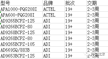
ACTEL, AD part advantageous ordering (operating the full range):
XILINX, ALTERA advantageous spot or ordering (operating the full range):
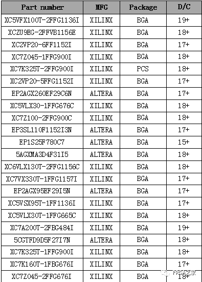
(The above devices are part of the models, for more models please consult the group owner Jin Juan)
Service concept: FPGA Home Component Self-operated City aims to facilitate engineers to quickly and conveniently purchase components. After several years of dedicated service, our customer service is spread across large listed companies, military research units, and small and medium-sized enterprises. Our biggest advantage is emphasizing service above all, and achieving fast delivery and favorable prices!
Directly operated brands: Xilinx, ALTERA, ADI, TI, NXP, ST, E2V, Micron and other hundreds of component brands, especially good at dealing with components subject to embargoes from Europe and the United States.We welcome engineer friends to recommend us to procurement or consult us directly!We will continue to provide the best service in the industry!

Official thanks to the brands of the FPGA technical group: Xilinx, Intel (Altera), Microsemi (Actel), Lattice, Vantis, Quicklogic, Lucent, etc.