Welcome FPGA engineers to join the official WeChat technical group.
Clickthe blue textto follow us at FPGA Home – the best and largest pure FPGA engineer community in China.

In summary, the power-up modes of Xilinx FPGA can be divided into the following 4 types:
Master Mode
Slave Mode
JTAG Mode (Debug Mode)
System Mode (Multi-Chip Configuration Mode)
Master Mode
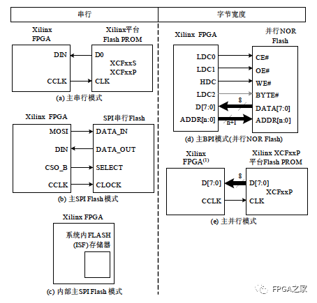
The typical master mode involves loading the configuration bitstream from external non-volatile (data retained after power-off) memory, with the clock signal required for configuration (called CCLK) generated internally by the FPGA, which controls the entire configuration process.
In master mode, after powering on, the FPGA automatically reads the configuration data from the corresponding external memory into SRAM, achieving internal structure mapping. Master mode can further be divided into serial mode (single bitstream) and parallel mode (byte-width bitstream) based on the bitstream width. For example: master serial mode, master SPI Flash serial mode, master parallel mode, etc.
Slave Mode
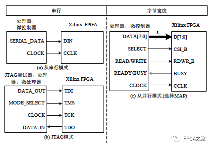
Slave mode requires an external master intelligent terminal (such as a processor, microcontroller, or DSP) to download data to the FPGA. Its biggest advantage is that the FPGA’s configuration data can be placed in any storage location in the system, including: Flash, hard disk, network, or even within the running code of other processors.
In slave mode, the FPGA acts as a subordinate device, with the corresponding control circuit or microprocessor providing the timing required for configuration to achieve data downloading. Slave mode can also be divided into serial and parallel modes based on the bitstream width.
JTAG Mode (Debug Mode)
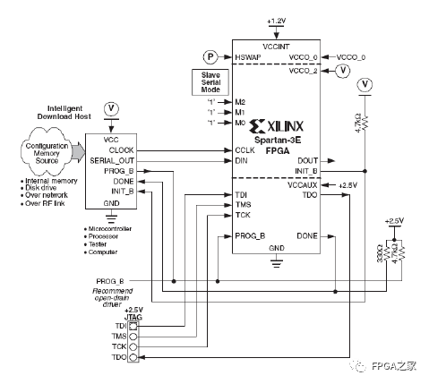
JTAG mode is a debug mode that allows the bit file stream from the PC to be downloaded to the FPGA, which is lost upon power-off. Xilinx’s FPGA chips feature a JTAG interface as specified by the IEEE 1149.1/1532 protocol. As long as the FPGA is powered on, regardless of the logic levels of the mode selection pins M[2:0], this configuration mode can be used. However, if the mode configuration pins are set to JTAG mode, i.e., M[2:0]=3’b101, then after powering on the FPGA chip or when a low pulse appears on the PROG_B pin, it can only be configured via JTAG mode.
In JTAG mode, the clock for communication between the PC and FPGA is the TCLK of the JTAG interface, with data entering the FPGA directly from TDI to complete the corresponding functional configuration.
System Mode (Multi-Chip Configuration Mode)
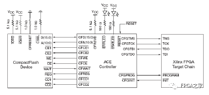
To address the configuration issues of large-scale FPGAs, Xilinx has introduced the system-level System ACE (Advanced Configuration Environment) solution. System ACE can configure all Xilinx FPGAs within a system or even across multiple boards, using Flash memory cards or micro hard disks to store configuration data, and transferring this data to the FPGA through the System ACE controller.
Appendix: System ACE’s CF (Compact Flash) Mode
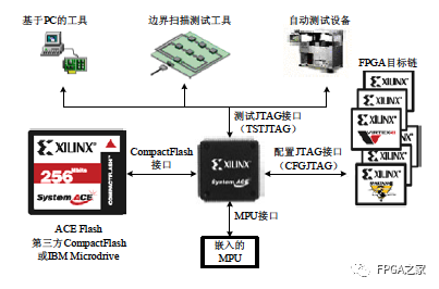
The System ACE CF storage devices include Xilinx’s ACE Flash cards or Compact Flash cards from other manufacturers, as well as IBM micro hard disks. The capacity of Compact Flash cards ranges from 32MB to 4GB, while micro hard disks range from 2GB to 6GB, allowing for the configuration of hundreds of FPGA chips.
The System ACE CF controller provides an interface between the storage unit and the FPGA device, as well as a standard JTAG interface between the PC and the memory. The default configuration mode of the controller chip is also to configure data into the FPGA chain via boundary scan, which can also assist in debugging system prototypes using the boundary scan chain’s testing and programming interface.

Welcome FPGA, embedded, signal processing engineers to follow our public account.

The largest FPGA WeChat technical group in the country
Welcome everyone to join the national FPGA WeChat technical group, which has tens of thousands of engineers and a group of technology-loving engineers. Here, FPGA engineers help each other, share knowledge, and foster a strong technical atmosphere!Hurry up and invite your friends to join!!

Press and hold to join the national FPGA technology group!
FPGA Home Components City
Advantageous component services, please scan the code to contact the group owner: Jin Juan Email: [email protected] Welcome recommendations to procurement.
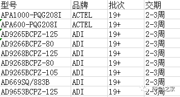
ACTEL, AD part advantages for ordering (full series):
XILINX, ALTERA advantages for immediate stock or ordering (full series):
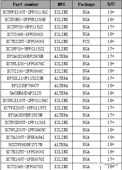
(The above components are partial models, for more models please consult the group owner Jin Juan)
Service philosophy: FPGA Home Components self-operated city aims to facilitate engineers in quickly and conveniently purchasing components. After years of dedicated service, our customer service is spread across large domestic listed companies, military research units, small and medium enterprises, and our biggest advantage is emphasizing the service-first philosophy, achieving fast delivery, and offering competitive prices!
Direct brand: Xilinx ALTERA ADI TI NXP ST E2V, Micron and over a hundred other component brands, especially skilled in components subject to US restrictions on exports to China.We welcome engineer friends to recommend us to procurement or consult us personally!We will continue to provide the best service in the industry!

Official acknowledgments from the FPGA technical group: Xilinx, Intel (Altera), Microsemi (Actel), Lattice, Vantis, Quicklogic, Lucent, etc.