This article mainly introduces the pin definitions, interface standards, boundary scan, and TAP controller of the JTAG bus.
JTAG (Joint Test Action Group) is an international standard testing protocol (IEEE 1149.1 compatible), primarily used for internal chip testing. Most advanced devices now support the JTAG protocol, such as ARM, DSP, FPGA, etc. The standard JTAG interface consists of 4 lines: TMS, TCK, TDI, and TDO, which correspond to mode selection, clock, data input, and data output lines, respectively.
Initially, JTAG was used for testing chips. The basic principle of JTAG is to define a TAP (Test Access Port) inside the device, allowing a dedicated JTAG testing tool to test internal nodes. JTAG testing allows multiple devices to be connected in series through the JTAG interface, forming a JTAG chain that enables individual testing of each device. Nowadays, the JTAG interface is also commonly used for implementing ISP (In-System Programmable) to program devices like Flash.
Internally, JTAG has a state machine called the TAP controller. The TAP controller’s state machine changes state through TCK and TMS, enabling data and instruction input.
1. Pin Definitions
There are many types of chips with JTAG interfaces, such as CPU, DSP, CPLD, etc. They all have the following JTAG pin definitions (signal direction is relative to the CPU):
-
TCK – Test Clock Input. Data from TMS and TDI is sampled on the rising edge of TCK. Data is output to TDO on the falling edge of the clock. It is recommended to pull down.
-
TDI – Test Data Input. Data input to the Instruction Register (IR) or Data Register (DR) appears at the TDI input and is sampled on the rising edge of TCK. It is recommended to pull up, with the pull-up resistor value not less than 1K.
-
TDO – Test Data Output. Data from the Instruction Register or Data Register is shifted out to TDO on the falling edge of the clock. No need for pull-up or pull-down; when floating, it should ideally be brought out as a test point, and TDO should not be used as an I/O.
-
TMS – Test Mode Select. TMS is used to set the JTAG interface into a specific test mode to control the TAP state machine. It must be pulled up.
-
VTref – Target Board Reference Voltage, connected to power. Used to determine the logic levels used by the CPU’s JTAG interface.
-
Optional Pin TRST – Test Reset, input pin, active low. TRST can be used to reset the TAP Controller (initialize). Since the TAP Controller can also be reset (initialized) through TMS, there is a distinction between 4-wire JTAG and 5-wire JTAG.
-
Optional Pin RTCK – Test Clock Return Signal. RTCK is the clock signal fed back from the target to the emulator, used to synchronize the generation of the TCK signal. When not used, it should be grounded.
-
Optional Pin nSRST – Target System Reset Signal. Connected to the system reset signal on the target board, it can directly reset the target system. It can also detect the reset status of the target system, and to prevent false triggering, appropriate pull-up resistors should be added on the target side.
-
TDIS
-
PD or TVD – (Presence Detect, Target Voltage Detect), similar to the function of VTref.
-
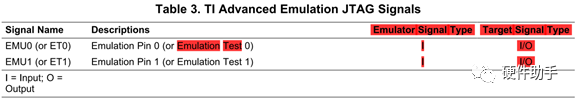
EMU[0:n] or ET[0:n] – (EMUlation, Emulation Test)
-
Boot Modes
-
Cross Triggers
-
Core Trace
-
System Trace
-
HS-RTDX (high speed RTDX, deprecated functionality)
2. JTAG Interface Standards
Currently, there are three standard connections for the JTAG interface: 10-pin, 14-pin, and 20-pin interfaces, defined as follows.
|
10-pin |
14-pin |
20-pin |
Pin |
Description |
|
2 |
13 |
2 |
VCC |
Power |
|
10 |
2,4,6,8,10,14 |
4,6,8,10,12,14,16,18,20 |
GND |
|
|
9 |
9 |
9 |
TCK |
Test Clock |
|
5 |
5 |
5 |
TDI |
Test Data Serial Input |
|
6 |
11 |
13 |
TDO |
Test Data Serial Output |
|
7 |
7 |
7 |
TMS |
Test Mode Select |
|
3 |
3 |
3 |
nTRST |
Test System Reset Signal |
|
4 |
12 |
15 |
nRESET |
Target System Reset Signal |
|
1 |
1 |
1 |
VTref |
Target Board Reference Voltage, connected to power |
|
8 |
11 |
RTCK |
Test Clock Return Signal |
|
|
17,19 |
NC |
★Since JTAG often uses ribbon cables for connections, to enhance anti-interference capability, ground lines are added between each signal line, and even numbered pins are ground signals.
3. Boundary Scan
The basic idea of boundary scan technology is to add a shift register unit near the input and output pins of the chip. Since these shift register units are distributed around the chip, they are called Boundary-Scan Register Cells.
When the chip is in debug mode, these boundary scan registers can isolate the chip from the peripheral inputs and outputs. Through these boundary scan register units, it is possible to observe and control the chip’s input and output signals. For the chip’s input pins, signals (data) can be loaded into the pins through the connected boundary scan register units; for the chip’s output pins, the output signals on those pins can be “captured” through the connected boundary scan registers. In normal operating conditions, these boundary scan registers are transparent to the chip, so normal operation is not affected. Thus, boundary scan registers provide a convenient way to observe and control the chips that need debugging. Moreover, the boundary scan (shift) register units on the chip’s input and output pins can be connected together to form a boundary scan chain around the chip. Generally, chips will provide several independent boundary scan chains to achieve complete testing functionality. The boundary scan chain can serially input and output, and through corresponding clock and control signals, it can easily observe and control the chip in debug mode.
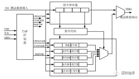
4. TAP (Test Access Port)
TAP is a universal port that allows access to all data registers (DR) and instruction registers (IR) provided by the chip. Control of the entire TAP is accomplished through the TAP Controller. TAP consists of 5 signal interfaces: TCK, TMS, TDI, TDO, and TRST; among them, 4 are input signal interfaces and 1 is an output signal interface. Generally, we see a JTAG interface on development boards, and the main signal interfaces of this JTAG interface are these five.
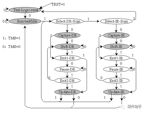
By keeping TMS high (logic 1) and inputting at least 5 gating pulses (going high and then low) at TCK, the TAP logic is reset. This transitions the TAP state machine from any other state to the Test-Logic Reset state, resetting the JTAG port and the test logic without resetting the CPU and peripherals.
The general process for accessing data registers (DR) through the TAP interface is:
-
Select a data register to access through the instruction register (IR).
-
Connect the selected data register between TDI and TDO.
-
Driven by TCK, input the required data into the selected data register via TDI; simultaneously, read the data from the selected data register via TDO.
-
The TAP controller’s state changes on the rising edge of TCK.
-
Upon power-up, it enters the Test-Logic Reset state, where all logic circuits of the test portion are disabled to ensure the normal operation of the chip’s core logic circuits. The TRST signal can also reset the test logic circuit, putting the TAP Controller into the Test-Logic Reset state. As mentioned earlier, TRST is an optional signal interface because applying 5 consecutive TCK pulse widths of “1” on TMS can also reset the test logic circuit, putting the TAP Controller into the Test-Logic Reset state. Therefore, the absence of the TRST signal will not have any effect.
-
Shift-DR state scans DR, and TDO output is valid.
-
Shift-IR state scans IR, and TDO output is valid.
-
In other states, TDO output is invalid.
If you need to capture the output on a pin of the chip, you first need to load the output on that pin into the boundary scan chain’s register unit, then output through TDO, allowing you to obtain the corresponding output signal from TDO. If you want to load a specific signal onto a certain pin of the chip, you first need to shift the desired signal into the boundary scan chain’s register unit connected to the corresponding pin via TDI, and then load the value of that register unit onto the corresponding chip pin.
The process for accessing the instruction register is: the system powers up, the TAP Controller enters the Test-Logic Reset state, then sequentially enters: Run-Test/Idle→Select-DR-Scan→Select-IR-Scan→Capture-IR→Shift-IR→Exit1-IR→Update-IR, and finally returns to the Run-Test/Idle state. In the Capture-IR state, a specific logical sequence is loaded into the instruction register; then it enters the Shift-IR state. In the Shift-IR state, driven by TCK, a specific instruction can be sent to the instruction register. Each instruction will determine a related data register. Then from Shift-IR→Exit1-IR→Update-IR. In the Update-IR state, the instruction just inputted into the instruction register will be used to update the instruction register. Finally, it enters the Run-Test/Idle state, the instruction takes effect, and the access to the instruction register is completed.
Accessing the data register: the currently accessible data register is determined by the current instruction in the instruction register. To access the data register selected by the previous instruction, you need to start from Run-Test/Idle, sequentially enter Select-DR-Scan→Capture-DR→Shift-DR→Exit1-DR→Update-DR, and finally return to Run-Test/Idle. During this process, the data register selected by the current instruction will be connected between TDI and TDO. Through TDI and TDO, new data can be loaded into the data register, and data in the data register can also be captured. The specific process is as follows. In the Capture-DR state, driven by TCK, the output signal on the chip’s pin will be “captured” into the corresponding boundary scan register unit. Thus, the current data register records the output signal on the corresponding chip pin. Next, transition from Capture-DR to Shift-DR state. In the Shift-DR state, driven by TCK, a new bit of data can be serially input into the data register through TDI in each clock cycle, while the data register can serially output a bit of previously captured data through TDO. After a number of clock cycles equal to the length of the data register, the input of the new signal and the output of the captured data can be completed. Then, transition from Exit1-DR state to Update-DR state. In the Update-DR state, the new data in the data register is loaded onto the chip pins connected to each register unit of the data register. Finally, return to the Run-Test/Idle state, completing the access to the data register.