Hello everyone, I am Pi Zi Heng, a serious tech enthusiast. Today, I will talk about the interface standard JTAG in embedded debugging.
In embedded development, it is inevitable to simulate and debug code, especially when the application logic becomes complex to a certain extent. It is common to introduce some logical bugs while writing code, and relying solely on code review may not eliminate all bugs. Therefore, online debugging becomes the most effective and direct way to eliminate bugs. Today, we will discuss the most fundamental aspect of debugging, which is the interface standard. The ARM core natively supports two industry-standard interface standards: JTAG and SWD. In this section, I will first explain the JTAG interface in detail.
1. JTAG Interface Standard
JTAG stands for “Joint Test Action Group,” which is both a standard and an organization. This organization was founded in 1985 by several major electronic manufacturers (IBM, AT&T, TI, Philips, etc.) with the purpose of initiating the formulation of a PCB and chip testing standard. The JTAG standard was approved by IEEE in 1990 as the IEEE1149.1 Test Access Port and Boundary Scan Architecture Standard. The JTAG standard specifies the hardware and software required for boundary scanning, primarily used for boundary scan testing of circuits and online system programming of programmable chips.
1.1 IEEE 1149.1 Standard
IEEE 1149.1 Working Group http://grouper.ieee.org/groups/1149/1/ Initial Manual 1149.1-1990 http://standards.ieee.org/findstds/standard/1149.1-1990.html Latest Manual 1149.1-2013 http://standards.ieee.org/findstds/standard/1149.1-2013.html
1.2 JTAG Interface Signals
The JTAG interface, collectively known as the Test Access Port (TAP), uses the following signals to implement boundary scan operations:
TCK (Test Clock): The clock signal that synchronizes the operation of the internal state machine.
TMS (Test Mode Select): The mode signal that controls the transition of the internal state machine (sampled on the rising edge of TCK).
TDI (Test Data In): The data that is shifted into the device for testing or programming logic (sampled on the rising edge of TCK).
TDO (Test Data Out): The data that is shifted out from the device for testing or programming logic (sampled on the falling edge of TCK).
In addition to the above signal lines, there is one optional signal:
TRST (Test Reset): The reset signal that resets the state machine of the TAP controller.
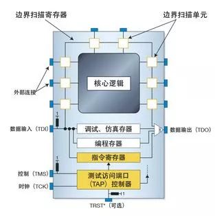
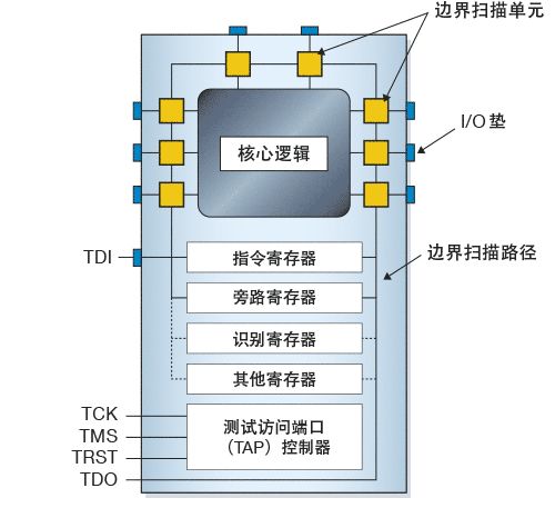
1.3 Internal Structure of JTAG System
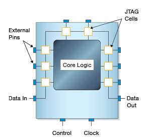
The most basic unit inside the JTAG system is the boundary scan unit (the values obtained from the scan are stored in the Boundary Scan Register (BSR)). Each boundary scan unit is located at the boundary of the target device, so JTAG testing is often referred to as boundary scan. All signals between the core logic of the target device and its pins are intercepted by a series of boundary scan units. Under normal operation, these boundary scan units are invisible. However, in test mode, these units can be used to set/read the values of the target device’s pins or core logic.
 |
 |
In addition to the above BSR, the JTAG system also requires the following three registers:
Instruction Register: Stores the current instruction, which is used by the TAP controller to determine how to process the received signals.
BYPASS Register: A unit register that transfers information from TDI to TDO.
IDCODE Register: Contains the identification code and version number of the device, which can associate the device with its Boundary Scan Description Language (BSDL) file.
The core of the JTAG system is the TAP controller, which is designed to interact with the internal registers of the JTAG system. The TAP controller is a synchronous state machine controlled by the TMS signal, which governs the behavior of the JTAG system. 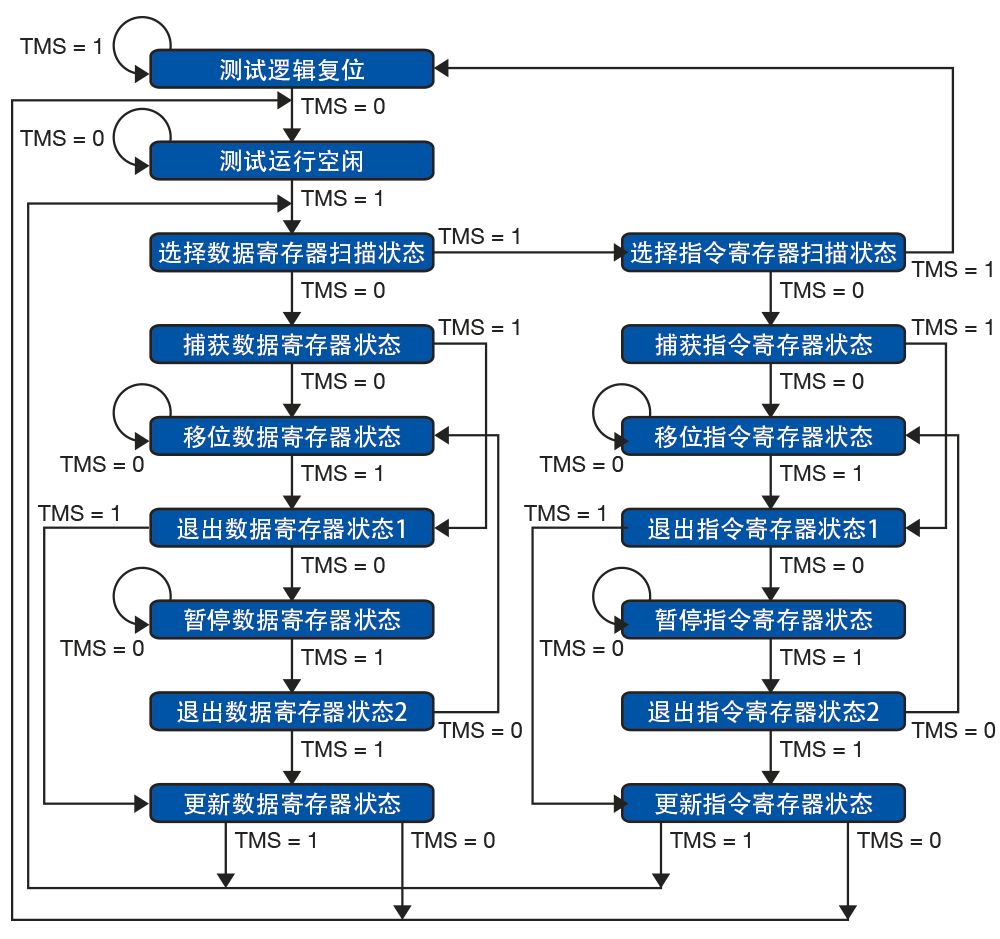 As shown in the figure above, the TAP controller’s internal state machine has a total of 16 states. For detailed meanings of each state, refer to the IEEE1149.1 manual. The basic function of the TAP controller is to generate the clock and control signals required for the normal operation of the BSR and instruction register. Its main functions include:
Providing signals to load instructions into the instruction register.
Providing signals to shift input data from the TDI pin into internal registers and to shift output data from internal registers to the TDO pin.
Executing corresponding functions, such as capture, shift, and update data.
The instruction register is used to store instructions that need to be interpreted and executed. The IEEE 1149.1 standard specifies the instructions that JTAG-compatible devices must have:
BYPASS: Transfers data using a single unit bypass register to shorten unnecessary scan links on the JTAG chain.
EXTEST: Drives known values (present in BSR) to the chip’s pins.
SAMPLE/PRELOAD: Loads captured values from the chip’s pins into the BSR.
In addition to the required instructions, the IEEE 1149.1 standard also specifies the following optional instructions:
IDCODE: Shifts out the data from the IDCODE register.
INTEST: Drives known values (present in BSR) to the chip’s core logic.
RUNBIST: When TAP enters the test run idle state, the chip performs self-testing.
1.4 JTAG Debug Tool Pinout
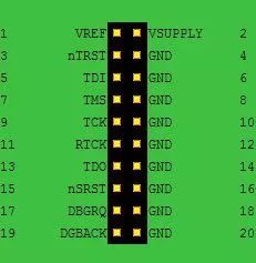
Typically, debugging and programming tools that support the JTAG interface actually utilize the four-wire TAP communication protocol of JTAG technology. Besides the standard TAP signal lines, other auxiliary signal lines are sometimes added to form a complete pinout. For ARM JTAG debugging tools, there are two commonly used pinout standards: ARM20 JTAG header and ARM14 JTAG header:
 |
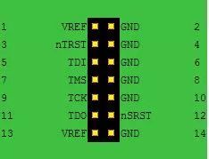 |
In the above two ARM JTAG headers, besides the standard TAP signal lines, the meanings of the other auxiliary signal lines are as follows:
| Signal Name | ARM20-pin | ARM14-pin | Signal Meaning |
|---|---|---|---|
| Vref | P1 | P1, P13 | JTAG interface reference voltage. Used to check whether the target system is powered, this pin is usually connected to the target system’s Vdd without any resistors in between. |
| Vsupply | P2 | N/A | Power input |
| nSRST | P15 | P12 | System Reset signal, connected to the target system’s reset signal. Can directly reset the target system and can also detect the reset status of the target system. To prevent false triggering, a suitable pull-up resistor should be added on the target side. |
| RTCK | P11 | N/A | Return Test Clock. Clock signal feedback from the target system to JTAG, used to dynamically control the TCK rate. Can be grounded when not in use. |
| GND | P4, P6, P8, P10, P12, P14, P16, P18, P20 | P2, P4, P6, P8, P10, P14 | Ground |
| DBGRQ | P17 | N/A | Connected to the target system’s debug request signal |
| DBGACK | P19 | N/A | Debug acknowledgment signal returned from the target system |
Note: For more JTAG pinout details, refer to the compilation on the JTAG test website http://www.jtagtest.com/pinouts/
2. JTAG Interface Advanced Topics
Having covered the basics of JTAG, I will now introduce some “black technologies” related to JTAG.
2.1 BSDL Files
Nowadays, more and more chips support the JTAG interface. To unify the specific JTAG implementations of various chip manufacturers and promote consistency in the entire electronics industry, the IEEE1149.1 standard has established the BSDL language specification. BSDL is the standard modeling language for JTAG devices, and its syntax is a subset of VHDL, describing the boundary scan characteristics of JTAG devices, mainly used to communicate between chip manufacturers, users, and testing tools.
Open-source JTAG BSDL library website (http://bsdl.info/), covering BSDL files of mainstream chips from major manufacturers
I randomly found a BSDL file for a chip (Freescale K60_1M (K24_144QFP)) for a simple analysis:
entity k60_1m is
     generic (PHYSICAL_PIN_MAP : string := "K24_144qfp");
-- Here describes the properties of all the chip pins
    port (
                                PTA0:        in   bit;
                                  ...
                              XTAL32:   linkage   bit);
    use STD_1149_1_2001.all;
    use STD_1149_6_2003.all;
-- Describe the chip pinout
    attribute COMPONENT_CONFORMANCE of k60_1m: entity is "STD_1149_1_2001";
    attribute PIN_MAP of k60_1m: entity is PHYSICAL_PIN_MAP;
    constant K24_144qfp :PIN_MAP_STRING :=
                                "PTA0:      50," &
                                   ...
                              "XTAL32:      40" ;
-- Describe the JTAG signal allocation on the chip pins
    attribute TAP_SCAN_OUT of PTA2 : signal is true;
    attribute TAP_SCAN_CLOCK of PTA0 : signal is (2.00e+07,BOTH);
    attribute TAP_SCAN_MODE of PTA3 : signal is true;
    attribute TAP_SCAN_IN of PTA1 : signal is true;
-- Describe the properties related to JTAG instruction registers
    attribute INSTRUCTION_LENGTH of k60_1m: entity is 4;
    attribute INSTRUCTION_OPCODE of k60_1m: entity is
        "BYPASS  (1111)," &
        "CLAMP  (1100)," &
        "EXTEST  (0100)," &
        "HIGHZ  (1001)," &
        "IDCODE  (0000)," &
        "PRELOAD  (0010)," &
        "SAMPLE  (0011)," &
        "ENABLE_CENSOR_CTRL  (0111)," &
        "ENABLE_TEST_CTRL  (0110)," &
        "EZPORT  (1101)," &
        "JTAGDP_ABORT  (1000)," &
        "JTAGDP_APACC  (1011)," &
        "JTAGDP_DPACC  (1010)," &
        "JTAGDP_IDCODE  (1110)";
    attribute INSTRUCTION_CAPTURE of k60_1m: entity is  "xx01";
    attribute INSTRUCTION_PRIVATE of k60_1m: entity is
        "ENABLE_CENSOR_CTRL," &
        "ENABLE_TEST_CTRL," &
        "EZPORT," &
        "JTAGDP_ABORT," &
        "JTAGDP_APACC," &
        "JTAGDP_DPACC," &
        "JTAGDP_IDCODE";
-- Describe the properties related to JTAG identification code registers
    attribute IDCODE_REGISTER of k60_1m: entity is
        "0000"  & -- Version
        "1011001100011010"  & -- Part Number
        "00000001110"  & -- Manufacturer Identity
        "1";  -- IEEE 1149.1 Requirement

    attribute REGISTER_ACCESS of k60_1m: entity is
        "BYPASS (BYPASS)," &
        "DEVICE_ID (IDCODE)";
-- Describe the properties related to JTAG boundary scan registers
    attribute BOUNDARY_LENGTH of k60_1m: entity is 196;
    attribute BOUNDARY_REGISTER of k60_1m: entity is
-- num cell   port/*                            function  safe  [ccell  dis  rslt]
"   0  (BC_2, *,                                control,  1)                       ," &
"   1  (BC_8, PTE0,                             bidir,    X,    0,      1,   Z)    ," &
...
" 194  (BC_2, *,                                control,  1)                       ," &
" 195  (BC_8, PTD15,                            bidir,    X,    194,    1,   Z)    ";
end k60_1m;
2.2 JTAG Daisy Chain
When your system has multiple JTAG devices, to solve the problem of excessive JTAG ports occupying PCB space, JTAG supports the following daisy chain connection method (especially widely used in FPGA applications):
 |
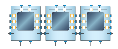 |
From the above figure, it can be seen that TMS and TCK are in a master-slave parallel structure (when there are too many devices, buffers (such as 74LVC245) need to be added to increase drive capability); TDI and TDO are in a master-slave series structure. This daisy chain method allows only one JTAG interface to access all JTAG devices on the PCB.
Thus, I have introduced the interface standard JTAG in embedded debugging. Where’s the applause~~~