In the ECU software development process, software debugging or testing often involves the JTAG interface, which is used through the JTAG protocol with emulators/debuggers such as JLink, ST-LINK, and Lauterbach for online debugging of software programs. Although many use it daily, not everyone is familiar with it. Therefore, this article intends to provide a brief introduction.
1 Overview of the JTAG Protocol
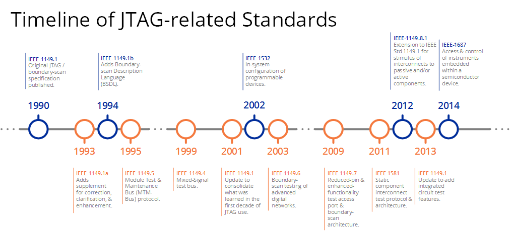
JTAG was established in the mid-1980s to develop a method for verifying designs and testing printed circuit boards after manufacturing. Before the development of JTAG, testing and debugging electronic circuits was a time-consuming and expensive process, as engineers had to manually probe and test each pin on the circuit board, which was not only slow but also prone to errors. The creation of JTAG aimed to provide a standardized interface for testing and debugging electronic circuits, using a set of special Test Access Ports (TAP) that allow engineers to interact with the circuit and perform various testing and debugging tasks.
-
The establishment of JTAG: In 1985, representatives from leading companies in the electronics industry, including Texas Instruments, IBM, Intel, and HP, formed the Joint Test Action Group. The main goal of this group was to create a standardized method for testing and debugging electronic systems, as traditional methods for testing these systems became increasingly complex and challenging. -
Early development and contributions: Key contributors to the early development of the JTAG protocol included Ken Parker from Texas Instruments, who proposed the concept of accessing multiple pins of an IC or PCB for testing through a single standardized interface. David Brownell from IBM made significant contributions to the design of the JTAG state machine, which plays a crucial role in controlling test operations and transitions. -
Introduction of the JTAG standard: In 1987, the Joint Test Action Group officially released the JTAG standard, namely IEEE 1149.1. This standard, titled “Standard Test Access Port and Boundary Scan Architecture,” provides a comprehensive framework for implementing the JTAG protocol in electronic devices. The JTAG standard defines the necessary signals and their functions, state machine operations, and boundary scan testing techniques. -
Rapid adoption and industry impact: The JTAG protocol quickly gained recognition in the electronics industry due to its numerous advantages. By providing a standardized testing method, JTAG greatly simplified the testing process for complex systems. It allows engineers to perform non-intrusive testing and debugging, even when physical access to individual pins is difficult or impossible. As a result, JTAG has become an indispensable part of the design, manufacturing, and testing processes for various electronic products. -
Evolution and expansion: With continuous technological advancements, the JTAG standard has evolved to meet the changing needs of the industry. Other standards and extensions have been introduced to enhance the capabilities of JTAG. For instance, IEEE 1149.4 addresses analog testing capabilities, while IEEE 1149.6 focuses on testing challenges in high-speed digital systems. -
Integration into industry standards: JTAG has been integrated into various other industry standards to further expand its range of applications and advantages. Notably, it has become part of IEEE 1500, which focuses on testing intellectual property (IP) cores within integrated circuits.
2 Architecture of the JTAG Protocol
-
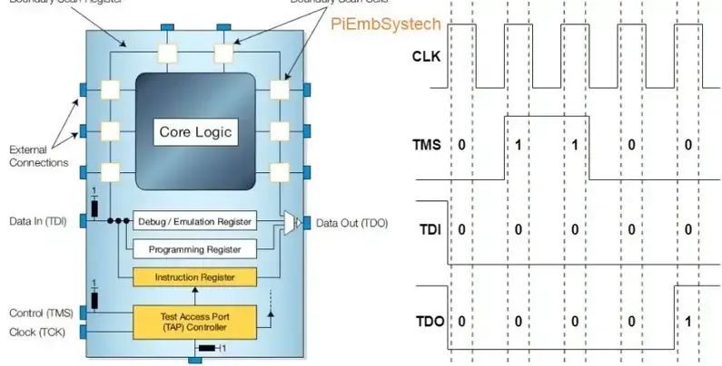
Test Clock (TCK): The clock signal that synchronizes data transfer between the testing device and the DUT.
-
Test Mode Select (TMS): The control signal that determines the state transitions of the TAP state machine.
-
Test Data Input (TDI): The bidirectional data signal used to input test data into the DUT.
-
Test Data Output (TDO): The bidirectional data signal used to output test data from the DUT.
-
Test Reset (TRST) (optional): The optional signal used to reset the TAP.
-
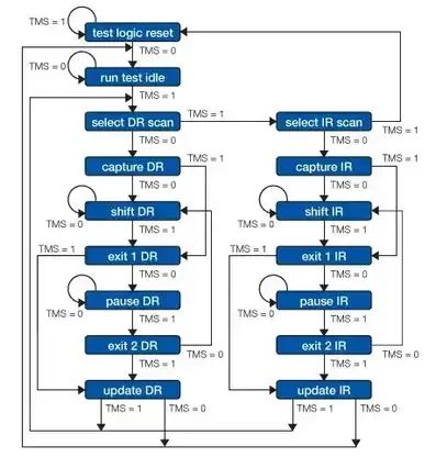
Test Logic Reset (TLR): The initial state after power-up or test reset, where the TAP remains in a stable state.
-
Run Test/Idle (RTI): The TAP is in an idle state, waiting for instructions or test data.
-
Select-DR-Scan (SDR): The state where the TAP is ready to shift data into or out of the DUT’s data register.
-
Capture-DR (CDR): The state that captures input data to be shifted into the DR.
-
Shift-DR (SDR): The state where data is shifted into or out of the DR.
-
Exit1-DR (EDR1): The state where the TAP exits the Shift-DR state, preparing for the next operation.
-
Exit2-DR (EDR2): The state where the TAP exits the Shift-DR state after the last bit has been shifted out.
-
EXTEST: The EXTEST instruction is used for interconnection testing. When activated, it connects the boundary scan register to the TDI and TDO, effectively putting the device into “external” test mode. In this mode, the boundary scan output units drive test data to the device pins, while the input units capture data from these pins. This instruction is critical for boundary scan testing. -
SAMPLE/PRELOAD: The SAMPLE/PRELOAD instruction is similar to EXTEST but allows the boundary scan device to maintain its task/function mode while still linking the boundary scan register to TDI and TDO. Using the SAMPLE/PRELOAD instruction, the boundary scan register can be accessed via data scanning while the device continues to operate. This feature is beneficial for preloading data into the boundary scan register without interrupting the device’s functional behavior, preparing it for subsequent execution of the EXTEST instruction. -
BYPASS: The BYPASS instruction establishes a direct connection between TDI and TDO through a single-bit register, bypassing the longer boundary scan register of the device, hence the name. BYPASS offers significant advantages in shortening the boundary scan chain by excluding devices that are not needed for the current operation. Devices receiving the BYPASS instruction maintain their task/function mode while allowing seamless serial data flow to subsequent devices in the chain.
4 JTAG Protocol TAP Controller
5 JTAG Connector and Pinout
-
20-pin JTAG connector. -
16-pin OCDS JTAG connector. -
14-pin JTAG connector. -
10-pin JTAG connector (ARM JTAG connector). -
Custom JTAG connectors. -
Surface-mount JTAG connectors. -
Flywire JTAG connectors.
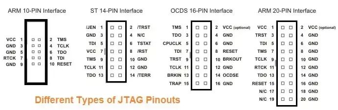
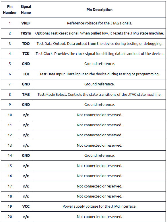
Taking the 20-pin JTAG connector as an example, the 20-pin JTAG connector is the most widely used. As the name suggests, it has 20 pins arranged in two rows of 10 each. This type of connector is commonly used in traditional JTAG applications and can be found on many development boards and evaluation platforms. It provides a standard interface for JTAG communication and is compatible with most JTAG programmers and debuggers. The pin definitions are as follows:
6 How the JTAG Protocol Works
-
Connect the JTAG hardware interface to the JTAG interface of the target device. -
Establish communication between the PC and the JTAG interface using the TCK, TMS, TDI, and TDO pins. -
Set the TAP to the desired state, such as Select-DR-Scan (SDR), to access and manipulate the internal registers of the device. -
Install the appropriate debugging software on the PC to connect to the target device via the JTAG interface. -
The debugging software allows you to read and write data to internal registers, set breakpoints, halt the processor, and perform other debugging operations.
7 Conclusion
Automotive R&D group chat, interested friends please add the group owner: prOmiseyes, and note: company + position to join the group. Limited to automotive industry professionals.