1. Introduction
Previously, we sharedhttps://mp.weixin.qq.com/s/BeL6UbSg2HI9qKemZugOhw?token=1054074707&lang=zh_CN
the article titled“Low-Cost Learning FPGA Based on“Mining Board”” which usesJTAG boundary scan for quick pin correspondence reverse engineering..
Not only forFPGAs, but we can also useJTAG for boundary scan testing inMCUs, provided that the corresponding chip supports this feature and the manufacturer providesBSDL files.
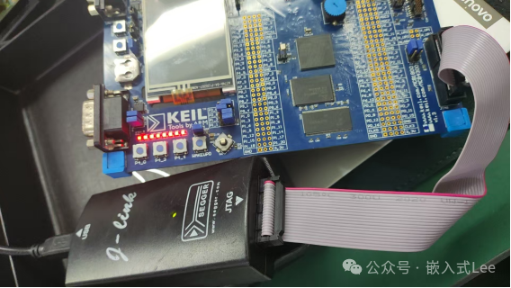
Here, we will demonstrate using theLPC1857 MCU, with the development board beingMCB1800.
As mentioned earlier, TopJTAG is a commercial software that requires purchase; here we provide a harmonious version for testing purposes only. If needed, please purchase the legitimate version to support it.
Files shared via cloud storage:TOPJTAG.zip
Link: https://pan.baidu.com/s/1ea_Bsyf4GIaqAfYheNlmhg?pwd=ybqc Extraction code: ybqc
—Shared by Baidu Cloud Super Memberv3.
2. Preparation
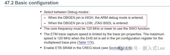
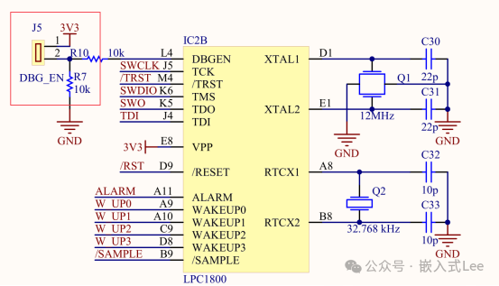
From the user manual, we can see that if theDBG_EN pin is pulled high, it is inARM debug mode, and if pulled low, it is inJTAG BSDL mode. We
will remove the jumper cap, thus pulling downDBG_EN to useJTAG BSDL mode. If you want to useJTAG to debug the simulation program, you need to short the jumper cap to pull upDBG_EN.
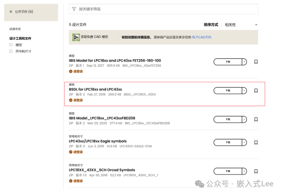
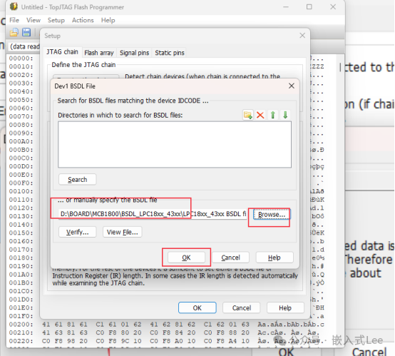
Download theBSDL file; login is required for download.
https://www.nxp.com.cn/products/LPC1857FET256
ConnectJINK, power on the development board.
3. Operation Process
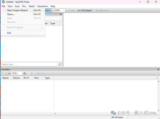
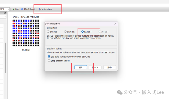
OpenTopJTAG Probe
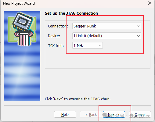
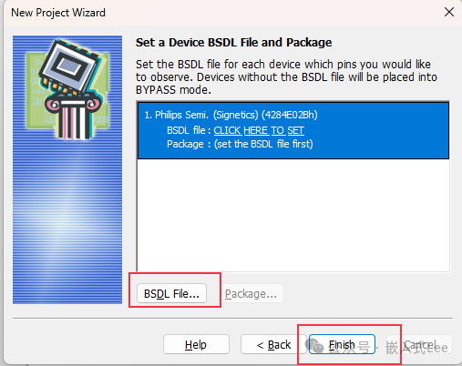
File->New Project Wizard
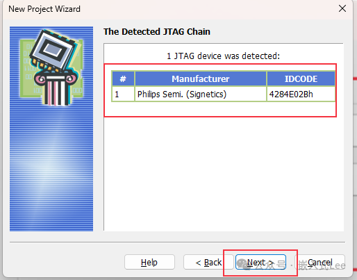
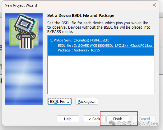
The chip is recognized, and theJTAG BSDL mode IDCODE is different from that of theARM DEBUG mode.
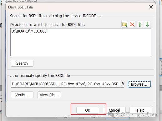
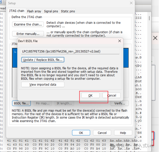
Select theBSDL file.
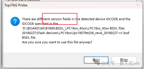
If the selectedBSDL file IDCODE is incorrect, a prompt will appear.
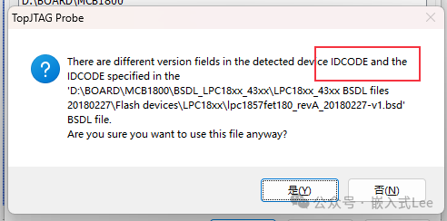
If the version selected is incorrect, a prompt will also appear.
You can directly open theBSDL file to see how the IDCODE is parsed.
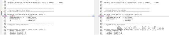
You need to select the correctIDCODE and the right version of theBSDL
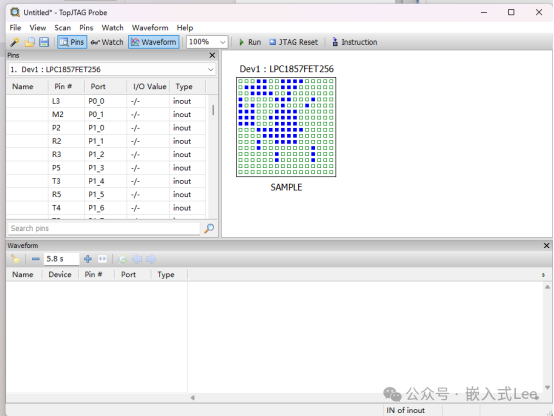
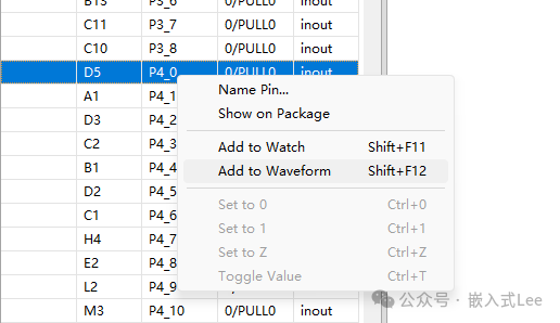
Taking the test key input as an example.
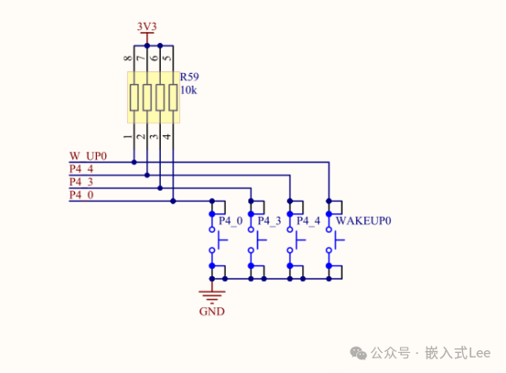
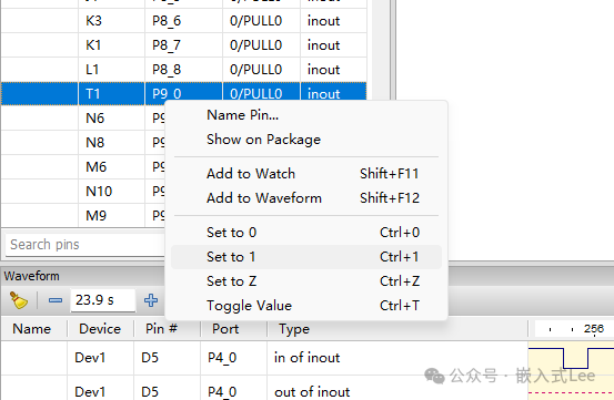
AddP40, P43, P44 to the waveform.
Clickrun
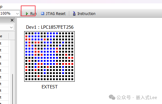
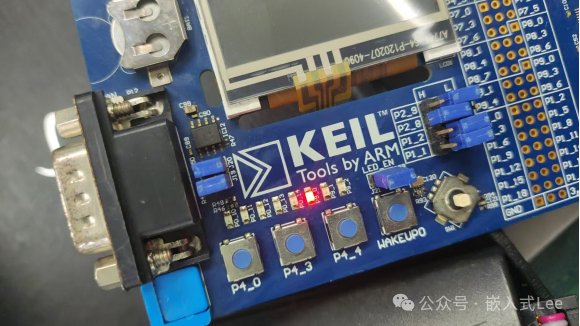
Press the button on the development board, and you can see the waveform change.
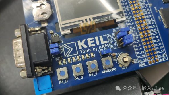
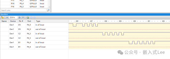
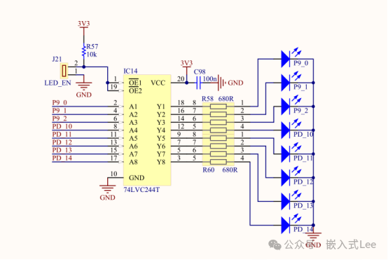
You can also directly control theLED, corresponding to the pins below, directly control the pin output to1 or 0, and see the LED turn on and off.
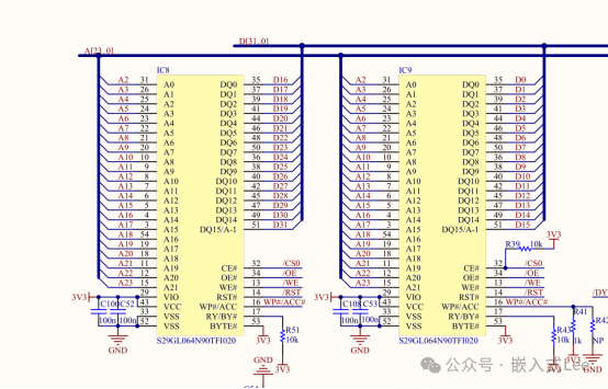
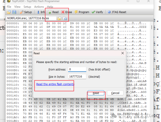
4. Read and WriteNOR
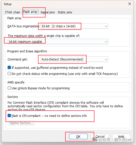
Two 8M 16-bitNOR FLASH chips form a 32-bit access, with a total capacity of16MB.
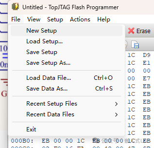
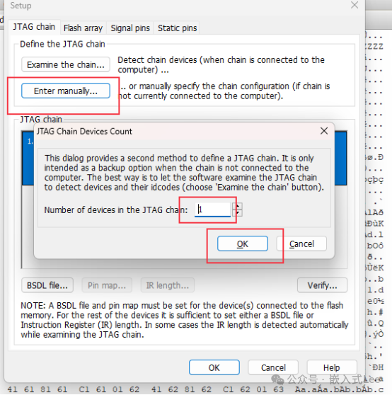
OpenTopJTAG Flash Programmer
File->New Setup
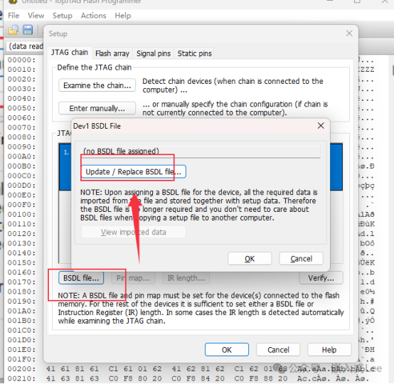
Set theFLASH properties.
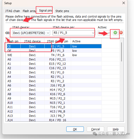
Set the pins.
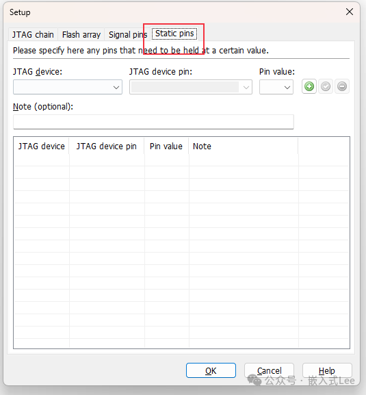
You can set certain pins to a fixed level, but it is not needed here.
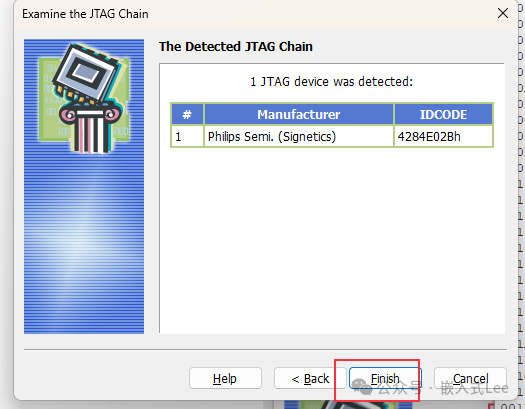
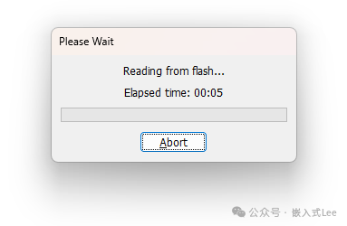
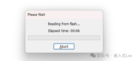
Start reading.
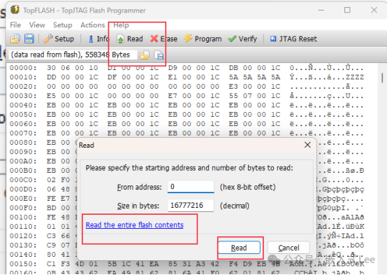
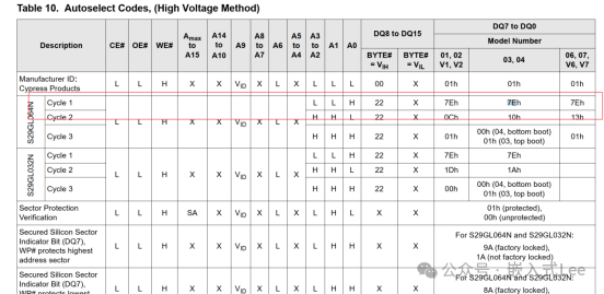
Info shows the deviceID
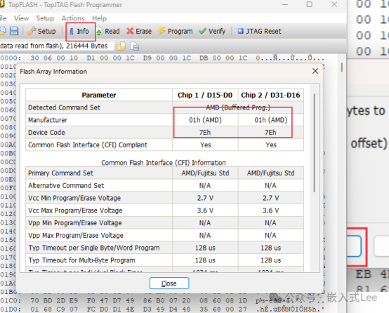
and corresponds to the manual.
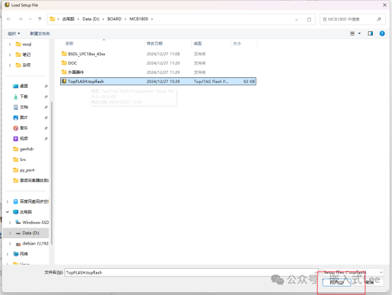
You canFile->Save Setup As… to save the environment for next time.
If you have already saved thesetup file, just load it directly.
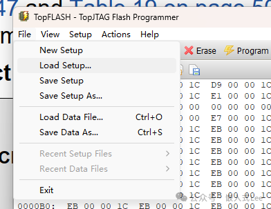
File-Load Setup
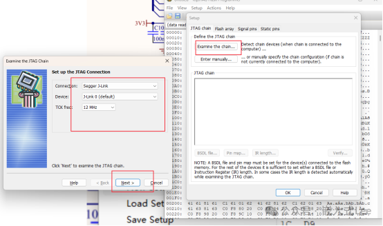
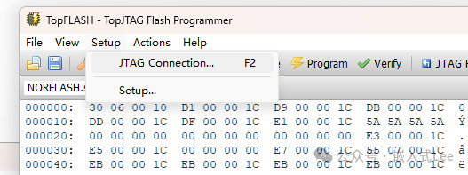
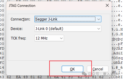
Setup->JTAG Connection…
5. Summary
UsingJTAG BSDL allows for quick testing of the chip. For example, upon receiving a development board, you can quickly test whether the corresponding pins’ input and output are correct, determining functionality faster than writing a program for testing. You can also directly control pins to read and writeFLASH. Here, TopFlash supports parallelNOR FLASH. In fact, we can write a host computer to support any protocol forFLASH, as we can directly manipulate any pin. For instance, the programming ofSPI FLASH throughJTAG in Vivado follows a similar principle. The advantage of usingJTAG for reading and writingFLASH is flexibility; however, the downside is that the speed is limited by theIO simulation speed, which depends on the speed ofJTAG, and the JTAG protocol consumes relatively more resources, making it generally slower.