Click the card below to follow Arm Technology Academy
This article is authorized to be transferred from the WeChat public account “Electronic Circuit Development Learning”. This article mainly shares content related to JTAG boundary scan.
How did I learn about boundary scan?
This starts with my purchase of an FPGA board.
Recently, I found an FPGA board on a second-hand platform, and it looks like this:
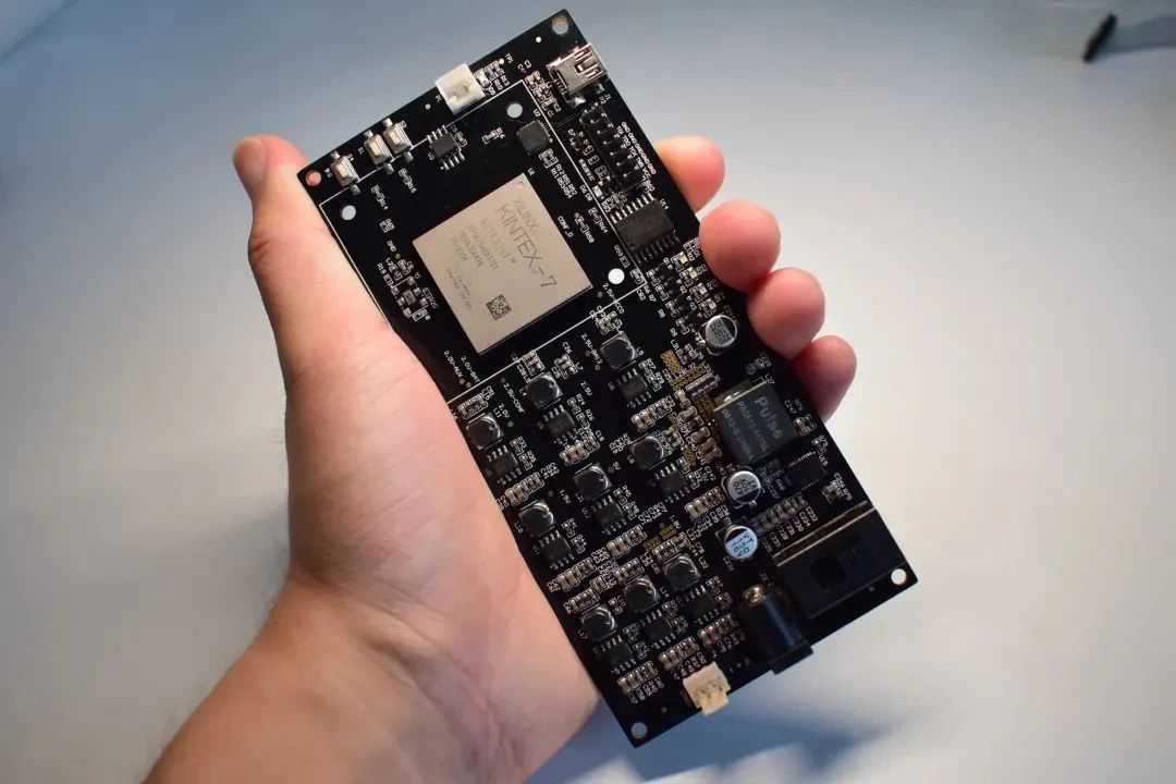
Figure 1
The overall size of the board is quite compact, about the size of a palm, and the peripherals are simple:
● 12V power supply with a heatsink.
● The FPGA chip is Xilinx XC7K325T, FFG676 package, chip grade 2I, production date is week 21 of 2017.
● 4-channel LED.
● 3 tactile buttons, one of which is Config.
● 1 CAN interface (without soldered CAN transceiver and level converter chip).
● 1 USB serial port, CP2102 conversion chip.
● 1 Spansion 128Mb QSPI Flash S25F128.
● 1 active differential clock 200MHz.
● Standard 2.54mm 14P download interface.
The seller told me that this was a HASH computing card from a customized mining machine during the mining boom, mainly functioning to receive data via serial port, calculate the HASH value using FPGA, and then output it via the serial port. Due to the high operating frequency, it also included a heatsink. Later, due to the mining crash, all cards from the mining machines were disposed of, unfortunately, no software or hardware documentation was left.
Fortunately, the price was quite cheap, only 150 yuan, knowing that just one FPGA chip costs more than 150 yuan.
After buying the board, I connected it to a 12V power supply, and the board lit up normally. The JTAG port was also functioning normally, and the FPGA chip was not encrypted, allowing for download and debugging. Although there was no large-capacity cache like DDR, making it impossible to perform complex calculations, even running MicroBlaze could not execute larger programs, but it was sufficient for learning the basic knowledge of FPGA, such as LED and button driving, serial port, CAN bus, SPI interface, and MicroBlaze SDK introductory learning.
Unfortunately, I did not know the pin definitions of the chip. The simplest and most brutal way is to use a hot air gun to remove the FPGA chip and then use a multimeter’s buzzer mode to determine the pin definitions of the LED, serial port, and other peripherals. This method carries a high risk; once removed and reinstalled, the board has a high risk of being scrapped.
So, is there a way to determine the pin definitions without damaging the board?
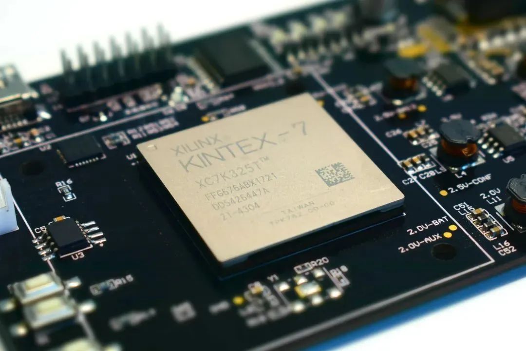
Figure 2
After some searching and inquiries, I found a method, which is JTAG boundary scan.
In simple terms, as long as you connect through the JTAG port, you can freely read or change the state of any pin of the chip.
For example, to obtain the pin corresponding to a button, you just need to hold and release the button, and then use boundary scan to check which pin of the FPGA has a state change to determine it; for the LED, although it is an output direction, we can also treat it as an input, artificially setting it to high or low through jumpers. In this way, the serial port pins, CAN pins, and clock pins can be identified one by one.
Next, I will guide you to roughly understand JTAG boundary scan in several parts, from the introduction of JTAG boundary scan, to the hardware and software of the upper computer, and then to the actual application of boundary scan based on MCU and FPGA.
1 What is Boundary Scan?
When it comes to boundary scan, we must mention JTAG, because boundary scan is one of the functions of the JTAG interface.
JTAG stands for Joint Test Action Group.
JTAG is very familiar to engineers in the electronics industry, whether they are working on microcontrollers, ARM development, or FPGA, DSP development, this interface is indispensable. It can not only download programs but also perform online debugging, completing such powerful functions with just a few wires, greatly improving development efficiency.
But did you know? The original intention of the JTAG protocol was not to download programs.
The ‘T’ in JTAG stands for Test. That’s right! The JTAG interface was originally designed for testing!
In the 1990s, as the integrated circuit and chip design industry began to develop rapidly, it also faced many problems: how to determine if the connections between chip pins and wafers are normal? Are there any short circuits between chip pins? After a chip is soldered onto a PCB, how can we ensure that the soldering is good, without short circuits or open circuits? How can we ensure that the peripheral circuits of the chip and the chips interconnected with it are functioning normally? Especially for some BGA packaged chips, direct measurement of the chip’s pins using probes and other methods is impossible.
In response to these issues, semiconductor manufacturers such as Philips and TI established the Joint Test Action Group, or JTAG, in 1985 to solve these problems.
Although people believe that the IEEE1149.1 standard is essentially JTAG, the official name of this standard is the Standard Test Access Port and Boundary-Scan Architecture. It defines the use of boundary scan to detect the Test Access Port (TAP) of PC circuit boards.
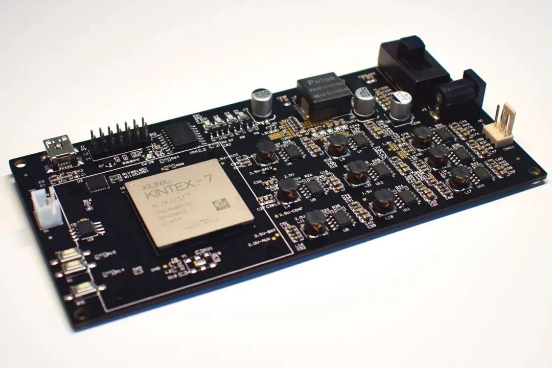
Figure 3
The JTAG protocol has developed to the point where there are currently three typical applications:
● Program downloading. This is the most commonly used function, which allows user programs to be downloaded into the chip’s internal Flash.
● Program debugging. This involves real-time monitoring of the program’s state and allows for real-time debugging by setting breakpoints.
● Boundary scan. This is the original intention of JTAG, mainly used for hardware testing of the chip itself and the PCB circuit board.
2 JTAG Hardware Interface
The basic logic of the JTAG protocol relies entirely on the internal TAP controller (Test Access Port), which is essentially a state machine that switches between different states using the TMS signal.
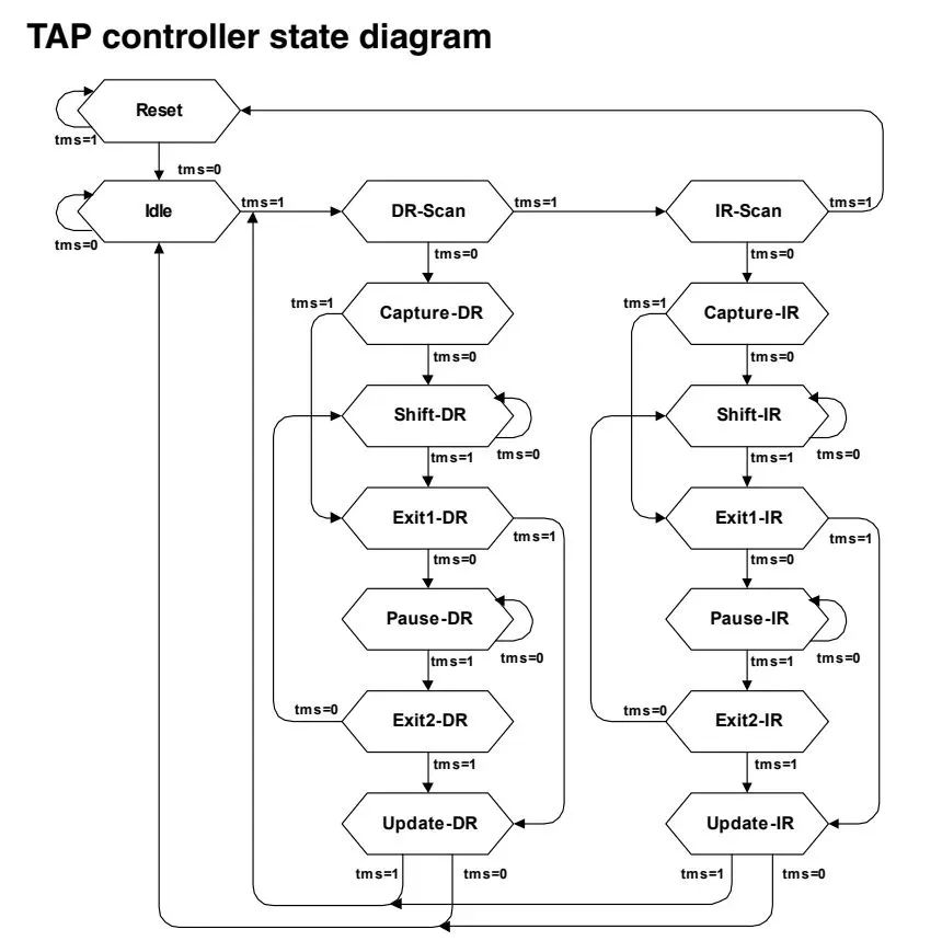
Figure 4
A standard JTAG interface requires at least four pins: TCK, TDI, TDO, and TMS. In the IEEE1149.1 standard, the TRST signal is optional.
Below are the definitions and functions of each signal:
● Test Clock Input (TCK)
TCK provides an independent, basic clock signal for the operation of the TAP, and all operations of the TAP are driven by this clock signal. TCK is mandatory in the IEEE1149.1 standard.
● Test Mode Selection Input (TMS)
The TMS signal is used to control the transitions of the TAP state machine. The TMS signal can control the TAP to switch between different states. The TMS signal is valid on the rising edge of TCK. TMS is mandatory in the IEEE1149.1 standard.
● Test Data Input (TDI)
TDI is the data input interface. All data to be input into a specific register is serially input bit by bit through the TDI interface (driven by TCK). TDI is mandatory in the IEEE1149.1 standard.
● Test Data Output (TDO)
TDO is the data output interface. All data to be output from a specific register is serially output bit by bit through the TDO interface (driven by TCK). TDO is mandatory in the IEEE1149.1 standard.
● Test Reset Input (TRST)
TRST can be used to reset (initialize) the TAP Controller. However, this signal interface is optional in the IEEE1149.1 standard and is not mandatory because TAP Controller can also be reset (initialized) through TMS.
For example, in the Jlink JTAG interface, you can see the standard four JTAG pins:
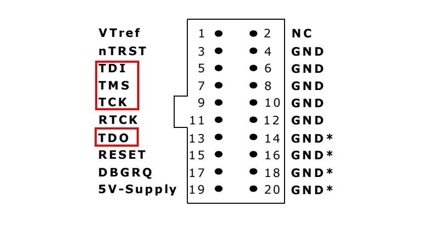
Figure 5
Below is a schematic of the use of the JTAG interface:
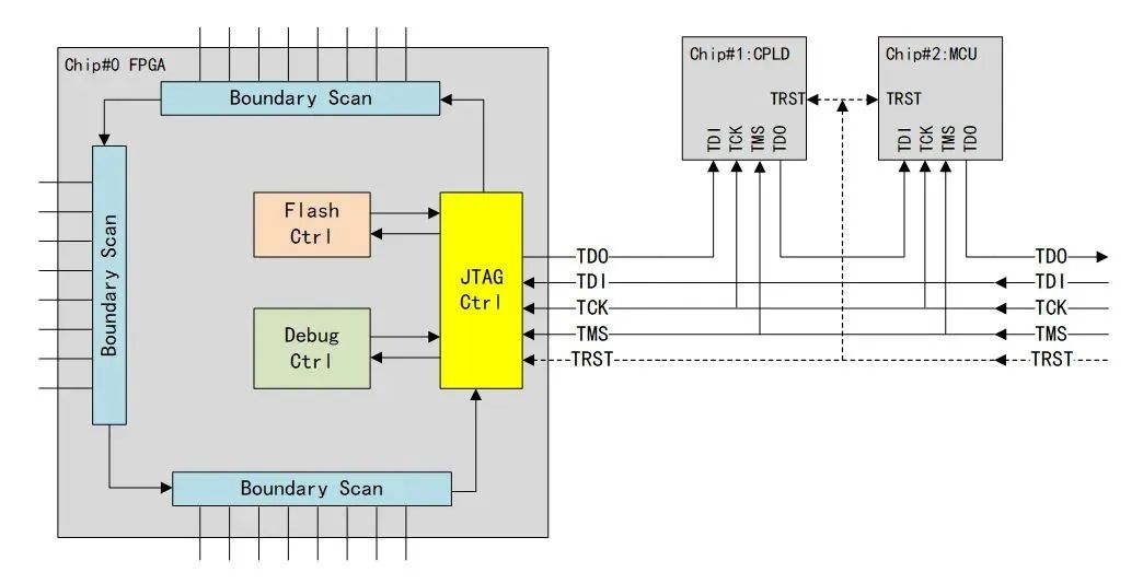
Figure 6
Each pin has a boundary scan register unit. Under the drive of the clock, the signals of each pin flow sequentially between the register units, enabling control and reading of the state of each pin.
3 Software and Hardware Related to Boundary Scan
Theoretically, any debugger or downloader that supports the JTAG protocol can be used for boundary scan testing, although it may require developing corresponding upper computer software.
This article introduces two common boundary scan testing solutions.
● JLink + TopJTAG Probe
TopJTAG is a very simple and practical boundary scan testing software that supports various debuggers, such as the most commonly used JLink, USB-Blaster, etc. I will introduce this software in conjunction with Jlink for boundary scan testing in a later article.
● X-JTAG
A very professional boundary scan solution, the development company is located in Cambridge, UK, including debuggers and upper computer, with extremely powerful functions, of course, at a high price! It is widely used in aerospace, automotive, defense, medical, communications, and other professional fields.
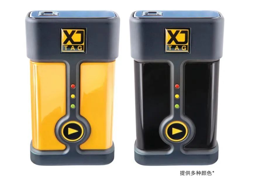
Figure 7
4 Learning Materials
A foreign guy posted a video on YouTube: EEVblog#449- What is JTAG and Boundary Scan, which has been uploaded on Bilibili, the address is:
● https://www.bilibili.com/video/BV1TT4y1e7HU
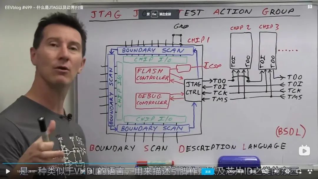
Figure 8
There is also a document titled “ARM JTAG Debugging Principles”, which is very concise, only 22 pages, providing a preliminary understanding of the JTAG protocol.
● http://www.micetek.com.cn/technic/jtag.pdf
The official document for the JTAG protocol is JTAG_IEEE-Std-1149.1-2001:
● https://fiona.dmcs.pl/~rkielbik/nid/JTAG_IEEE-Std-1149.1-2001.pdf
Although it is not the latest version, it is sufficient as a reference for learning the JTAG protocol.
5 Conclusion
By the way, the board I introduced at the beginning, I obtained the pin definitions through boundary scan as follows:
##################################################################### Copyright(C), 2010-2023, https://blog.csdn.net/whik1194# ModuleName : top.xdc # Date : 2023-03-04# Time : 23:55:00# Author : whik1194# Function : Pin constraint# Version : v1.0# Version | Modify# ----------------------------------# v1.0 first version####################################################################set_property PACKAGE_PIN AA10 [get_ports gclk_p]set_property PACKAGE_PIN D9 [get_ports greset]set_property PACKAGE_PIN D8 [get_ports key]set_property PACKAGE_PIN G20 [get_ports led1]set_property PACKAGE_PIN H19 [get_ports led2]set_property PACKAGE_PIN E20 [get_ports led3]set_property PACKAGE_PIN F19 [get_ports led4]set_property PACKAGE_PIN F8 [get_ports uart_rxd]set_property PACKAGE_PIN F9 [get_ports uart_txd]set_property PACKAGE_PIN G14 [get_ports can_rx]set_property PACKAGE_PIN H14 [get_ports can_tx]set_property IOSTANDARD DIFF_SSTL12 [get_ports gclk_p]set_property IOSTANDARD DIFF_SSTL12 [get_ports gclk_n]set_property IOSTANDARD LVCMOS33 [get_ports greset]set_property IOSTANDARD LVCMOS25 [get_ports led1]set_property IOSTANDARD LVCMOS25 [get_ports led2]set_property IOSTANDARD LVCMOS25 [get_ports led3]set_property IOSTANDARD LVCMOS25 [get_ports led4]set_property IOSTANDARD LVCMOS33 [get_ports key]set_property IOSTANDARD LVCMOS33 [get_ports uart_rxd]set_property IOSTANDARD LVCMOS33 [get_ports uart_txd]set_property IOSTANDARD LVCMOS33 [get_ports can_rx]set_property IOSTANDARD LVCMOS33 [get_ports can_tx]#QSPI set_property BITSTREAM.GENERAL.COMPRESS TRUE [current_design]set_property BITSTREAM.CONFIG.CONFIGRATE 50 [current_design]set_property BITSTREAM.CONFIG.SPI_BUSWIDTH 4 [current_design]If any friends have also purchased this board, feel free to exchange and learn from each other!
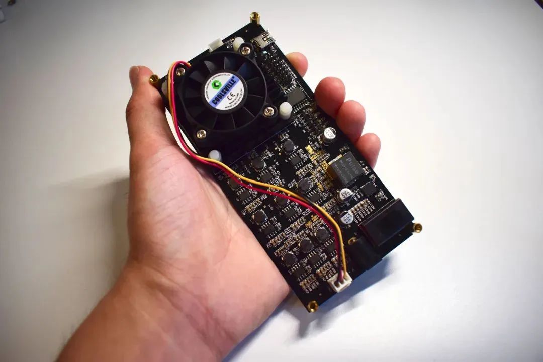
Figure 9
Recommended Reading
-
FPGA Automation Execution in Linux
-
Overview of Intelligent FPGA Network Cards (1): PISA + Rocket
-
Starting from thirty years ago, a comprehensive introduction to the evolution of FPGA architecture!


Long press to recognize the QR code to add Miss Ji’s WeChat (aijishu20) and join the Arm Technology Academy reader group.
Follow Arm Technology Academy
 Click the button below “Read the original text” to read more articles about electronic circuit development learning.