For embedded developers and hardware hackers, JTAG is the standard for debugging and accessing microprocessor registers. This protocol has been in use for many years and is still used today. The JTAG debugging interface requires VCC, GND power signals, and four debugging signals: TMS, TCK, TDI, and TDO. Additionally, TRST and RESET reset signals and RTCK (synchronous clock) signals are optional. As devices become smaller, the number of available pins on microprocessors decreases, and these complex signals hinder the normal use of the protocol.
To address this issue, ARM created an alternative debugging interface called SWD (Serial Wire Debug). Compared to the JTAG interface, SWD uses fewer signals, utilizing only two signals (SWDCLK and SWDIO). This interface and its associated protocol are now used in almost all Cortex-[A,R,M] processors.
Cortex-A: Application processor cores for performance-intensive systems, Cortex-A processors provide a range of solutions for devices utilizing operating systems (such as Linux or Android), which are used in various applications, from low-cost handheld devices to smartphones, tablets, set-top boxes, and enterprise networking equipment.
Cortex-R: High-performance cores for real-time applications, the Cortex-R series is the smallest ARM processor among derivatives. Cortex-R processors are targeted at high-performance real-time applications, such as hard disk controllers (or solid-state drive controllers), networking devices and printers in enterprises, consumer electronics (such as Blu-ray players and media players), and automotive applications (such as airbags, braking systems, and engine management). The Cortex-R series is similar in some ways to high-end microcontrollers (MCUs), but it targets larger systems than those typically using standard MCUs.
Cortex-M: Microprocessor cores for various embedded applications, the Cortex-M series is aimed at the highly competitive MCU market. The Cortex-M series is built on the ARMv7-M architecture (used for Cortex-M3 and Cortex-M4), while the lower Cortex-M0+ is based on the ARMv6-M architecture. The first Cortex-M processor was released in 2004, and as some mainstream MCU suppliers adopted this core and began producing MCU devices, the Cortex-M processor quickly gained market favor. It can be said that Cortex-M is to 32-bit MCUs what the 8051 is to 8-bit MCUs, supported by numerous suppliers as an industrial standard core, with various suppliers adopting this core along with their unique developments to provide differentiated products in the market.
 ARM Debug Interface
Architecture Overview
Unlike JTAG, which links interfaces together, SWD uses a bus called DAP (Debug Access Port). On this DAP, there is a master port (DP – Debug Port) and one or more slave ports (AP – Access Port), similar to the JTAG interface. DP handles transactions with AP using packets containing AP addresses.
In summary, external debuggers connect to the DAP using the SWD protocol through the DP, and ARM’s introduction provides a good overview of the SWD architecture:
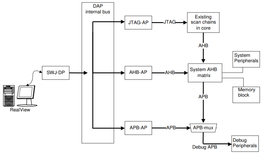
SWD Architecture
Debug Port
The debug port is the interface between the host and the DAP, and it also handles the host interface. Currently, there are three different debug ports available to access the DAP:
JTAG debug port (JTAG-dp): This port uses the standard JTAG interface and protocol to access the DAP;
Serial Wire Debug port (SW-DP): This port accesses the DAP using the SWD protocol;
Serial Wire/JTAG debug port (SWJ-DP): This port can access the DAP using either JTAG or SWD. This is a common interface on many microprocessors. It reuses the TMS and TCK JTAG signals to transmit SWDIO and SWDCLK signals, respectively. To switch from one interface to another, a specific sequence must be sent.
Access Ports
Multiple APs can be added to the DAP as needed. ARM provides specifications for two APs:
1. Memory Access Port (MEM-AP): This AP provides access to core memory and registers;
2. JTAG Access Port (JTAG-AP): This AP allows a JTAG chain to connect to the DAP.
 SWD Protocol
Signals
As mentioned earlier, SWD only uses two signals:
· SWDCLK: The clock signal sent by the host. Since there is no relationship between the processor clock and the SWD clock, the frequency choice depends on the host interface. In this article, the maximum debugging clock frequency is approximately 60MHz.
· SWDIO: This is a bidirectional signal that transfers data from DP to DP. Data is set by the host on the rising edge and sampled by DP on the falling edge of the SWDCLK signal. In digital circuits, the moment when the digital level changes from low (digital “0”) to high (digital “1”) is called the rising edge. The moment when the digital level changes from high (digital “1”) to low (digital “0”) is called the falling edge.
Transaction Processing
Each SWD exchange process consists of three phases:
1. Request phase: 8 bits sent from the host port;
2. ACK phase: 3 bits sent from the target port;
3. Data phase: Up to 32 bits sent to or from the host port, with a parity bit;
Note that a Trn cycle must be sent when the data direction changes.
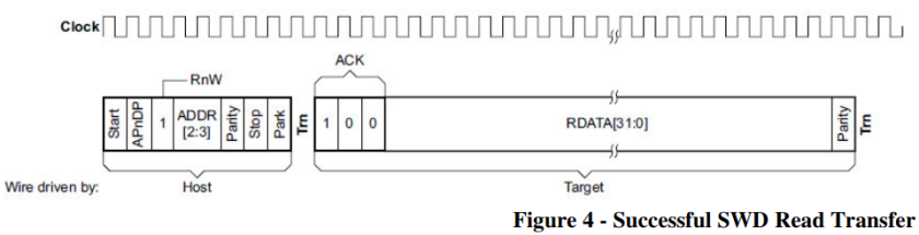
SWD Transfer
Request
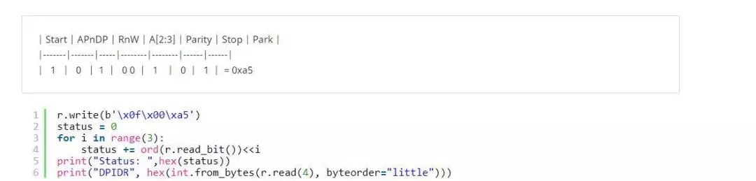
The request header contains the following fields:
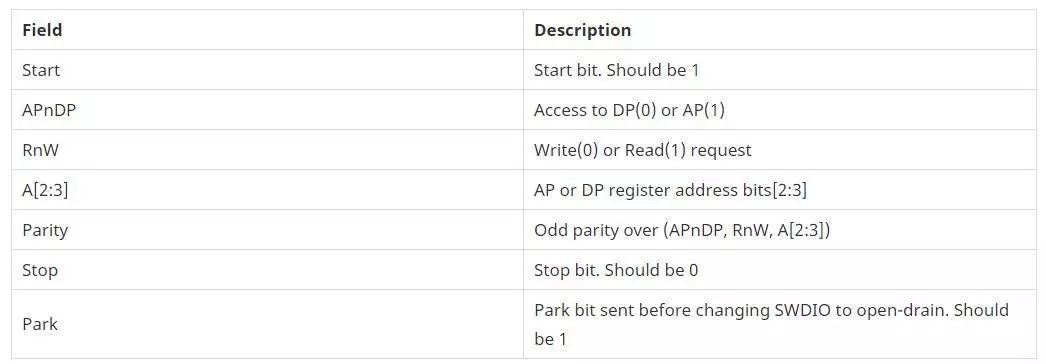
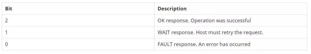
ACK
ACK (Acknowledgement) is a control character sent from the receiving station to the sending station in data transactions, indicating that the data received is confirmed to be correct.
In the TCP/IP protocol, if the receiver successfully receives the data, it will reply with an ACK data. Typically, the ACK signal has a fixed format and length, which is sent from the receiver to the sender.
The ACK bit contains the ACK status of the request header. Note that the three bits in the LSB must be read first.
Data
Data is sent from the host or the target. It first sends the LSB and ends with a parity bit.
 Protocol Interaction
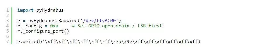
Now that we understand the lower-level parts of the protocol, it’s time to interact with the actual target. To do this, I used Hydrabus, but tools like Bus Pirate or any other similar tools can also be used. The Bus Pirate is a hardware hacking Swiss Army knife designed and produced by Dangerous Prototypes, supporting multiple common protocols and being cross-platform (Windows/Linux/MAC) with rich documentation.In this article’s tests, I used a development board called Blue Pill based on STM32F103.The nickname Blue Pill (blue pill rootkit is a malicious software that executes as a hypervisor to control computer resources) was presented by Joanna Rutkowska, a security researcher at the Singapore IT security company COSEIN, during her presentation at the Black Hat briefing in 2006. The Blue Pill rootkit was developed as a proof-of-concept malware.The original blue pill operation is based on AMD virtualization (AMD-V), which is a set of hardware extensions for the X86 processor architecture.This processor extension offloads redundant and inefficient work from software.By processing these tasks through processor extensions, traps, and virtualization emulation, tasks bypass the operating system, significantly improving the performance of virtual machines on physical servers.
The ARM Debug Interface Architecture Specification document contains all the details required to interact with the SWD interface, and here is the specific process:
SWD Initialization
Since the target uses the SWJ-DP interface, it needs to switch from the default JTAG mode to SWD. Chapter 5.2.1 of the specification document shows the sequence for switching from JTAG to SWD:
1. Drive SWDIOTMS HIGH for at least 50 SWCLKTCK cycles to ensure the current interface is in a reset state. The JTAG interface only detects the 16-bit JTAG-to-SWD sequence starting from the Test-Logic-Reset state.
2. Send the 16-bit JTAG-to-SWD selection sequence on SWDIOTMS;
3. Drive SWDIOTMS HIGH for at least 50 SWCLKTCK cycles to ensure that if the SWJ-DP was already in SWD operation before sending the selection sequence, the SWD interface enters line reset state.
0b0111 1001 1110 0111 (0x79e7) MSB sequence priority, we need to use LSB-first format of 0x7b 0x9e.
Now that the DP is in reset state, we can issue a DPIDR read command to identify the debug port. For this, we need to read the DP register at address 0x00.
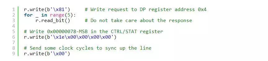
The next step is to activate the debug domain. Chapter 2.4.5 of the specification document tells us to set CDBGRSTREQ and CDBGRSTACK (bits 28 and 29) in the DP’s CTRL/STAT (address 0x4) register:
 SWD Usage
Now that the debug power domain is activated, the DAP can be fully accessed. As the first discovery process, we will query the AP and then scan all APs in the DAP.
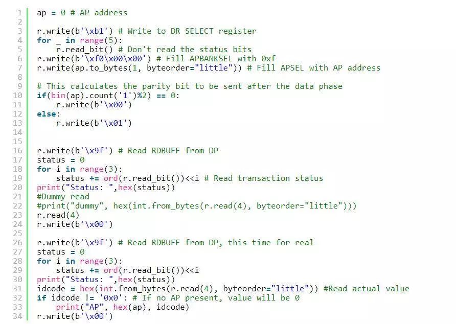
Reading AP
Reading data from the AP is done through the DP. To query the AP, the host must tell the DP which AP is specified by the address on the DAP. To read data from the previous transaction, the DP uses a special register called RDBUFF (address 0xc). The correct query method is as follows:
1. Write to the DP SELECT register to set the APSEL and APBANKSEL fields;
2. Read the DP RDBUFF register to “commit” the last transaction;
3. Again read the RDBUFF register to read its actual value.
The SELECT register is described in Chapter 2.3.9, with key fields as follows:
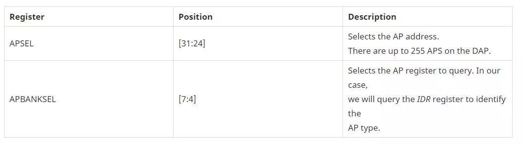
An interesting AP register to read is the IDR register (address 0xf), which contains identification information for this AP. Below is the code for reading the IDR of the AP at address 0x0.
Scanning AP
Using the exact same code, we can iterate through the entire address space to see if there are any other APs on the DAP:
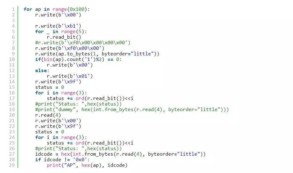
Running the script shows that there is only one AP on the bus. According to the specification document, it is the MEM-AP:
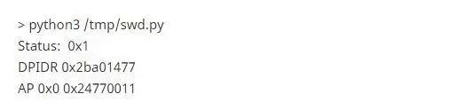
At this point, you can send commands to the MEM-AP to query the processor memory.
 Finding SWD Pins
On real devices, determining which pins or test points are used for the debug interface is not always easy. The same goes for JTAG, which is why tools like JTAGulator exist. Its purpose is to discover JTAG interfaces by trying every pin combination until a valid IDCODE (Identity code) is returned. Currently, a good tool for finding JTAG pins is JTAGULATOR, an automated tool for discovering JTAG pins.
Now that we understand how to initialize the SWD interface, we can perform the same operations on the SWD interface. The idea is as follows:
1. Use some interesting pins on the target board;
2. Connect them to the SWD discovery device;
3. Select two pins on the SWD discovery device, designated as SWDCLK and SWDIO;
4. Send the SWD initialization sequence;
5. Read the status response and DPIDR register;
6. If the result is valid, print the solution;
7. If there is no valid result, return to step 3 and select two new pins.
Through practical testing, this method has been implemented on Hydrabus firmware and has achieved good results. The following is a session example:
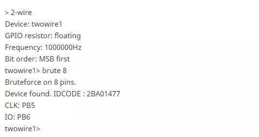
This operation takes less than two seconds and has successfully discovered the SWD interface on all tested boards.
 Conclusion
In this article, we introduced how to design the ARM debug interface and how the SWD protocol works at a very basic level. With this information, you can send queries to the MEM-AP using a simple microprocessor.