1. IntroductionSPI (Serial Peripheral Interface) is a high-speed, full-duplex synchronousserial communication bus protocol developed by Motorola, operating in a master-slave mode, enabling data transmission between devices through four lines (SCLK, MOSI, MISO, CS). Its core features are:① Full-duplex communication: Data can be transmitted in both directions simultaneously, allowing both the master and slave devices to send/receive data;② High-speed data transmission, supporting high data rates (up to several Mbps);③ Low power consumption: Reduces power consumption through clock synchronization mechanisms;④ Flexible expansion: Supports multiple slave devices through chip select signals (CS) to select the target device.SPI is widely used inindustrial control,embedded systems and other fields, such as connecting OLED displays, wireless modules, and other peripheral devices.2. Signal Definitions
① MISO (Master Input Slave Output): Data input from the master device, data output to the slave device;
② MOSI (Master Output Slave Input): Data output from the master device, data input to the slave device;
③ SCLK (Serial Clock): Clock signal generated by the master device;
④ CS/SS (Chip Select/Slave Select): Slave device enable signal controlled by the master device. In a master-slave configuration, CS/SS is the control signal indicating whether the slave chip is selected by the master chip. The master chip’s operations on the slave chip are only valid when the chip select signal is at the predetermined enable level (high or low).
One-to-one communication circuit: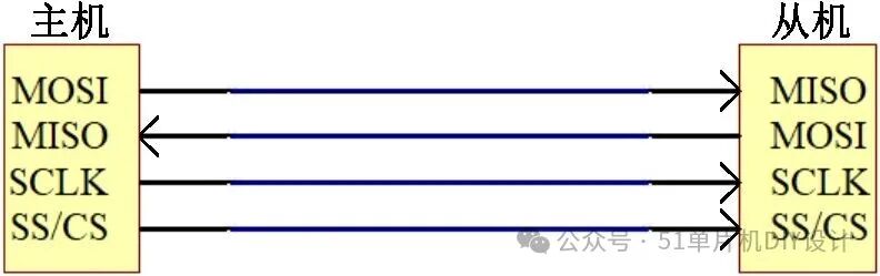
One-to-many communication circuit:
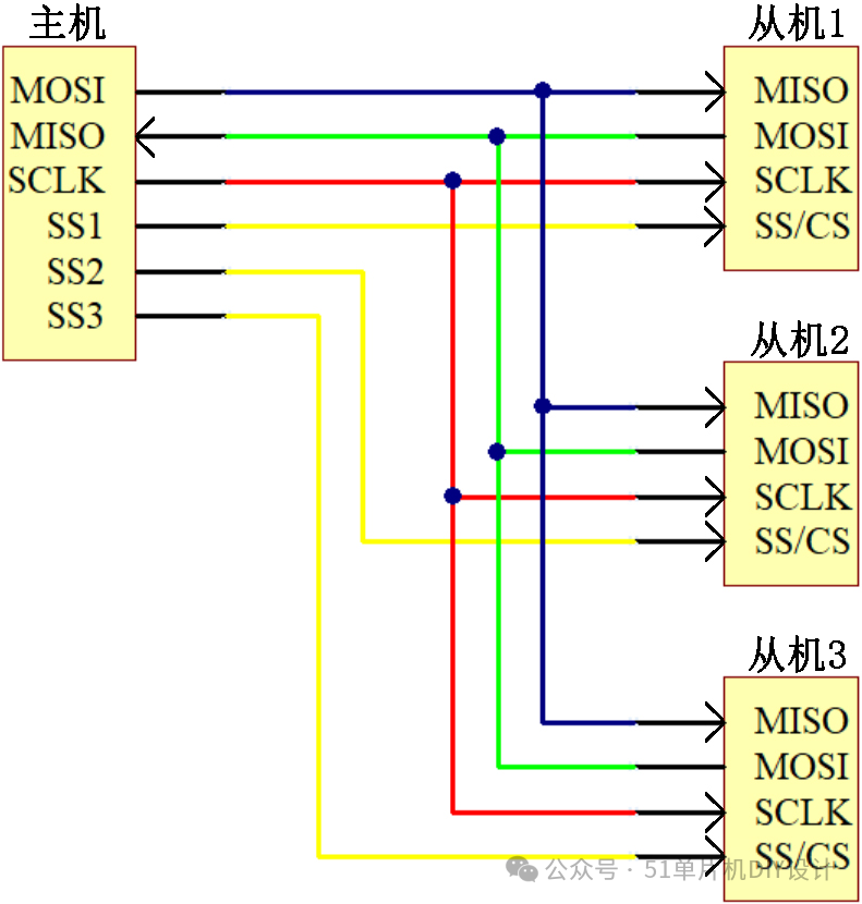 3. Communication Protocol
Both the SPI master and slave devices are designed with a serial shift register. The master device initiates a transmission by writing a byte to its SPI serial register. Data transmission and reception occur synchronously, hence it is also referred to as a full-duplex serial communication protocol.
SPI only distinguishes between master mode and slave mode, without a concept of read and write. The write and read operations of peripherals are completed synchronously. If only data writing is required, the master can ignore the received data (virtual); conversely, if the master only needs to read data from the slave, it must send a virtual byte of data to trigger the slave to transmit data. In simpler terms, sending data will result in receiving data, and receiving data requires sending data first.
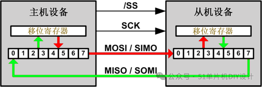
The process of SPI data communication can be divided into the following steps:
① The master initiates a signal by pulling CS/SS low to start communication.
② The master sends clock signals to trigger the slave to perform write or read operations (the sampling timing may be on the rising edge (low to high) or falling edge (high to low) of the clock signal, as SPI has four modes, which will be discussed later). It will immediately read the signal on the data line, thus obtaining one bit of data (1bit).
③ The master writes the data to be sent into the transmit buffer (Memory), which passes through the shift register (the buffer length may vary depending on the microcontroller configuration). The serial shift register transmits the byte bit by bit to the slave via the MOSI signal line, while the data received through the MISO interface is shifted into the receive buffer bit by bit.
④ The slave also returns the contents of its serial shift register (buffer length may vary depending on the microcontroller configuration) to the master via the MISO signal line. Simultaneously, it receives the data sent by the master through the MOSI signal line, thus exchanging the contents of the two shift registers.
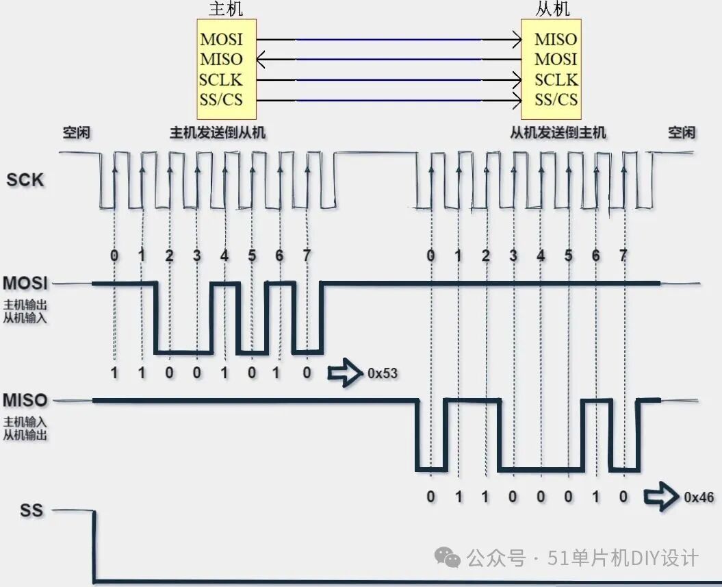
Pulling the SS chip select signal low starts communication and generates clock signals. The rising edge triggers the edge signal, and the master sends data 0X53 bit by bit on the MOSI line while receiving data 0X46 bit by bit on the MISO line.
4. Communication Characteristics
① Device Selection:
SPI is a single master communication protocol, meaning only one master device can initiate communication. When the SPI master device wants to read/write to a slave device, it first pulls the corresponding SS line of the slave device low (SS is active low). It then begins sending working pulses to the clock line, during which the master sends signals to MOSI to achieve “write” while sampling MISO to achieve “read.” As shown in the figure below:
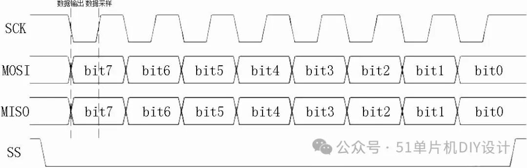
② Device Clock
The characteristics of the SPI clock mainly include: clock rate, clock polarity, and clock phase.
③ Clock Rate
The master on the SPI bus must configure and generate the corresponding clock signal at the start of communication. Theoretically, as long as it is practically feasible, the clock rate can be any rate you desire, although this rate is limited by the maximum system clock frequency each system can provide and the maximum SPI transmission rate.
④ Clock Polarity
Depending on the naming conventions of hardware manufacturers, clock polarity is usually denoted as CKP or CPOL. Clock polarity and phase together determine how data is read, such as whether data is read on the rising or falling edge of the signal.
CKP can be configured to 1 or 0. This means you can set the default state (IDLE) of the clock to high or low as needed. Polarity inversion can be achieved through simple logic inverters. You must refer to the device’s datasheet to correctly set CKP and CKE.
CKP = 0: Clock idle state is low (0);
CKP = 1: Clock idle state is high (1).
⑤ Clock Phase
Depending on the hardware manufacturer, clock phase is usually denoted as CKE or CPHA. As the name suggests, clock phase/edge refers to whether data is sampled at a specific phase or edge of the clock signal;
CKE = 0: Data is sampled on the first transition edge of the clock signal SCK;
CKE = 1: Data is sampled on the second transition edge of the clock signal SCK.
⑥ Four Modes
Based on the characteristics of SPI clock polarity and clock phase, four different SPI communication operation modes can be set. Their differences define which edge of the clock pulse toggles the output signal, which edge samples the input signal, and the stable level of the clock pulse (whether the clock signal is high or low when inactive). Details are as follows:
Mode 0: CKP=0, CKE=0: When idle, SCK is low; data is sampled on the first edge, which is the transition from low to high of SCK, so data is sampled on the rising edge (preparing data), and data is sent on the falling edge.
Mode 1: CKP=0, CKE=1: When idle, SCK is low; data is sent on the second edge, which is the transition from low to high of SCK, so data is sampled on the falling edge, and data is sent on the rising edge.
Mode 2: CKP=1, CKE=0: When idle, SCK is high; data is sampled on the first edge, which is the transition from high to low of SCK, so data is sampled on the falling edge, and data is sent on the rising edge.
Mode 3: CKP=1, CKE=1: When idle, SCK is high; data is sent on the second edge, which is the transition from high to low of SCK, so data is sampled on the rising edge, and data is sent on the falling edge.