Today, Xinyan Electronics, a one-stop PCBA processing manufacturer, will discuss the role of SPI inspection in SMT processing and its significance.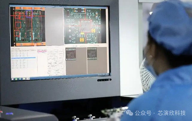
1. How SPI Becomes the “Eye of Fire” on SMT Production Lines
SPI (Solder Paste Inspection) solder paste inspection machines, which may seem like ordinary metal enclosures, house a precision optical system. Unlike traditional two-dimensional inspection equipment, the laser triangulation technology used can achieve a vertical resolution of ±1μm, which is equivalent to detecting a thickness change of 1/70 of a human hair. When the PCB printed with solder paste enters the inspection chamber, the high-speed scanning head completes a three-dimensional modeling of the 0402 component pads (0.5mm×0.25mm) within 0.8 seconds.
A quality report from a military electronics company showed that after introducing SPI, the defect rate of QFN packaged components dropped from 3‰ to 0.2‰. This improvement stems from SPI’s precise control over solder paste volume—when the system detects insufficient solder on a pad, it immediately triggers compensation for the printer parameters, preventing the risk of open circuits after reflow soldering.
2. A Quality Management Revolution from Firefighting to Prevention
In 2018, a certain automotive electronics manufacturer recalled due to cold solder joints in ECU modules, with the root cause analysis revealing that solder paste was missing due to stencil blockage. Following this incident, the industry began to widely adopt online SPI inspection. Today’s advanced SPI systems have achieved three major breakthroughs:
1. Dynamic Tolerance Compensation: Automatically matching inspection standards based on component types, such as a solder paste thickness tolerance of ±15μm for QFN devices, while relaxing it to ±25μm for BGA.
2. Trend Warning Mechanism: By analyzing statistical process control (SPC), early warnings are issued when parameters exceed the 2σ range, preventing batch anomalies.
3. Data Traceability System: Archiving the three-dimensional data of solder paste for each PCB, allowing for cross-analysis with subsequent AOI and X-ray inspection results.
Practices from a certain foundry have shown that this preventive inspection has improved the CPK value of the printing process from 1.0 to 1.67, meaning the defect rate dropped from 2700 PPM to 64 PPM.
3. The Hidden Cost-Benefit Equation
On the surface, an imported SPI device requires an investment of 800,000 to 1,500,000 yuan, but savvy production managers calculate a different equation: for an SMT line with a monthly output of 500,000 points, the introduction of SPI can lead to:
– A 40% reduction in the pick-and-place machine’s waste rate.
– A 65% reduction in repair labor hours after reflow soldering.
– An 80% decrease in customer return costs.
More importantly, the big data accumulated from SPI solder paste printing is changing the process optimization model. A certain company found through analyzing 12 months of historical data that for every 10% increase in environmental humidity, the solder paste diffusion area increases by 3%. The compensation model established based on this has reduced seasonal quality fluctuations by 70%.
4. Invisible Assessment Indicators for Choosing Foundries
When customers audit suppliers, in addition to focusing on the brand of the pick-and-place machine, they should also examine the depth of SPI application. High-quality foundries’ SPI systems often possess:
- Closed-loop control that interacts in real-time with the MES system.
- The capability to inspect 01005 components (0.4mm×0.2mm).
- A process parameter database that can be traced back over three years.
A certain medical device manufacturer was issued a 483 observation during an FDA audit due to incomplete SPI data chains from their foundry. This warns us that SPI is not just a testing tool but an important digital infrastructure for quality systems.
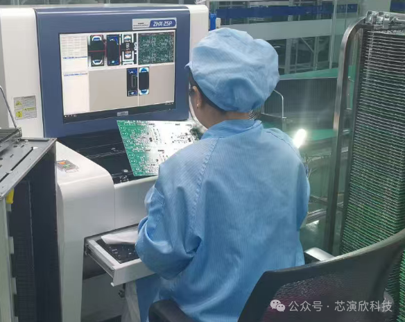
With the trend of miniaturization in electronic products, 0201 components and 0.35mm pitch BGAs have become the norm. When the pad area shrinks to 0.2mm², a solder paste deviation of 0.01mm³ can lead to soldering failures. The existence of SPI has transformed SMT processing from an experience-driven “craft” into data-driven precision manufacturing. It acts like a genetic testing device for solder paste quality, eliminating potential defects before component placement, which is the essential path for modern electronic manufacturing to achieve zero defects.