Previous article, introduced the JTAG boundary scan application based on STM32F103, demonstrated the application of TopJTAG Probe software, and the basic functions of boundary scan. This article introduces the boundary scan application based on Xilinx FPGA, which is almost the same.
1. Obtain the Chip’s BSDL File
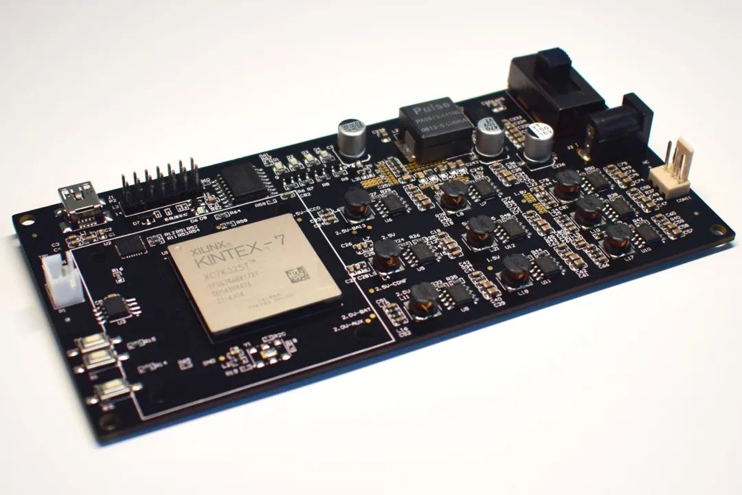
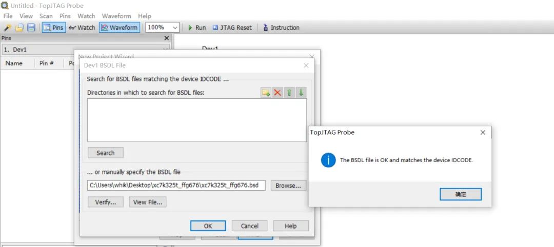
The method of obtaining the BSDL file for FPGA can refer to the previous article: Obtaining BSDL Files.Taking the Xilinx Kintex-7 series FPGA XC7K325T as an example, it can be obtained from the BSDL Library website (www.bsdl.info ) or from the installation directory of ISE and Vivado,
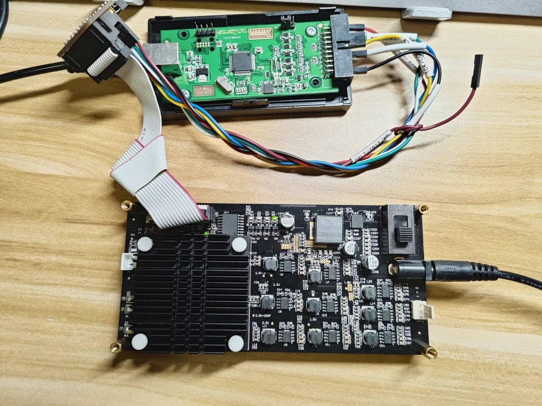
The JTAG interface of Xilinx and the JLink JTAG interface have different pin sequences, so separate dupont wires are needed to connect TCK, TMS, TDI, TDO, and VREF, GND signals.
3. Boundary Scan Testing
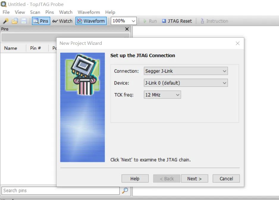
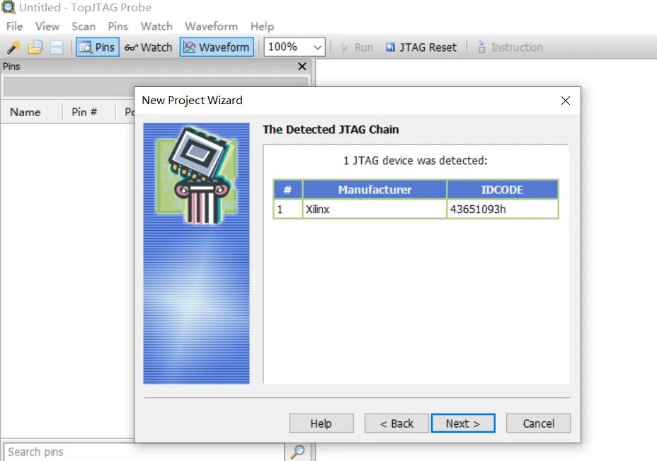
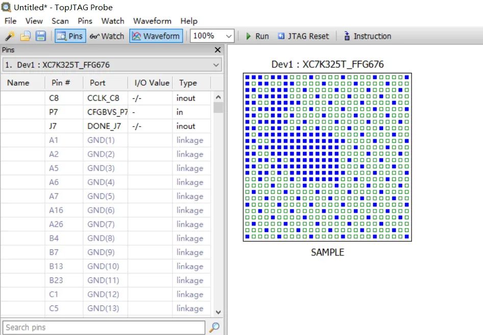
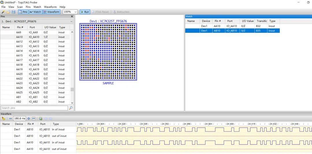
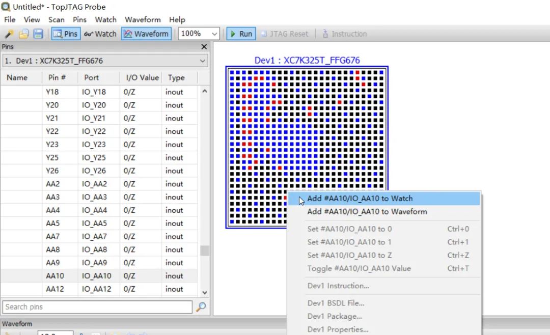
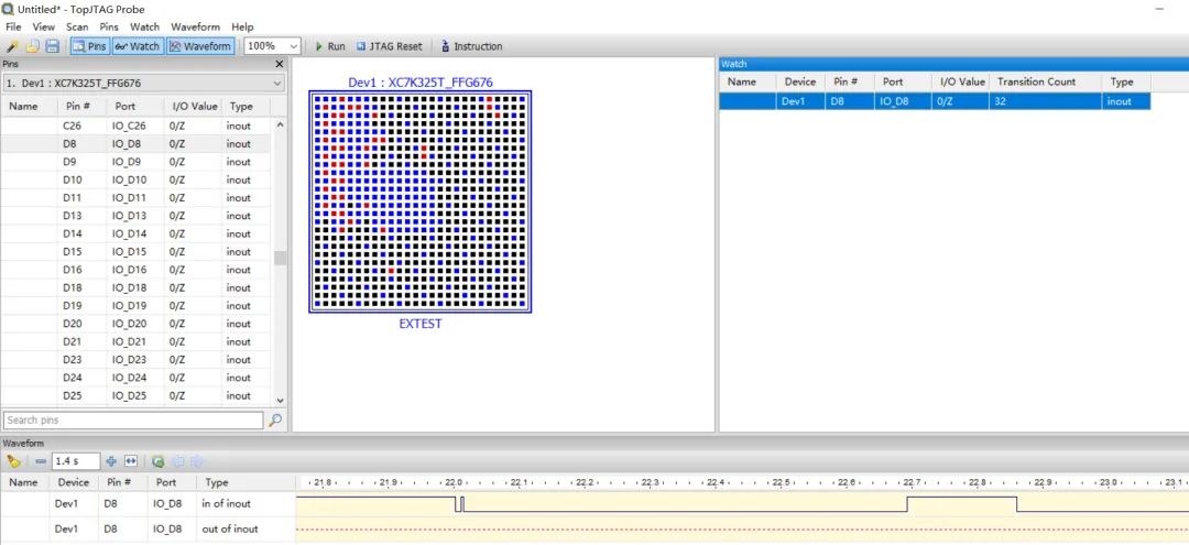
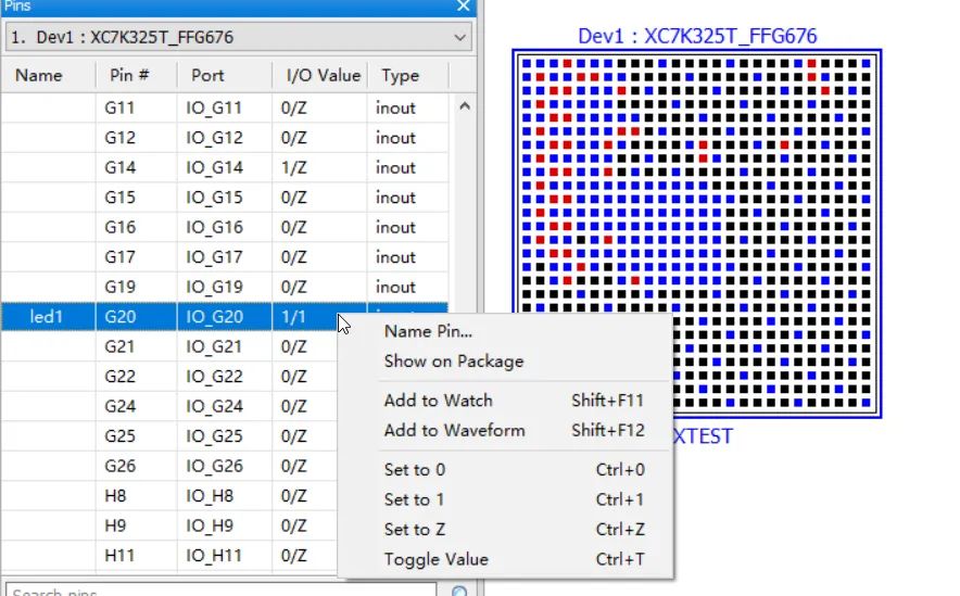
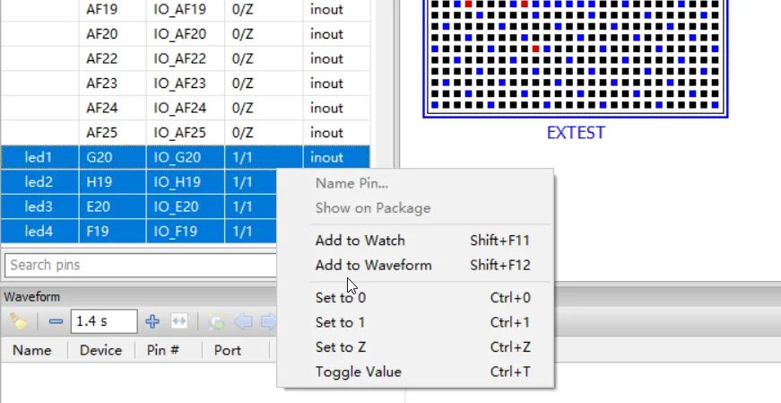
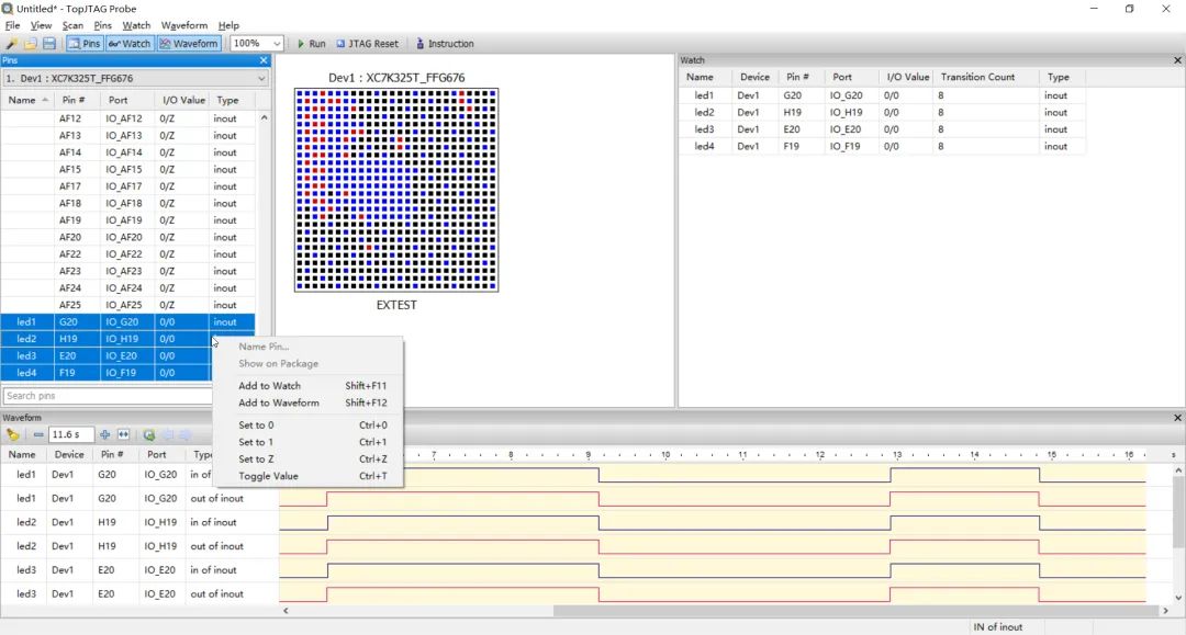
Open TopJTAG to create a new project, select JTAG device as JLinkIf the connection is normal, the IDCODE of the currently connected chip will be displayedSpecify the BSDL file path and perform IDCODE verification.The initial state is stop state,The initial default is Sample state, click the RUN button to see the real-time status of all pins, black indicates power pins, black indicates high level, blue indicates low level. Flashing indicates that the current state is high-low level flip state.In the left Pins window or the right chip view, select a chip pin, right-click, and you can choose to add it to the Watch window or Waveform windowThe Watch window can see the real-time status of the pins and can count the number of level flips, the Waveform window can display real-time waveforms.The Waveform supports basic operations such as zooming in, zooming out, and pausing.In the Pins window, after selecting a pin and right-clicking, you can name it, output high, low level, or high impedance state.Support batch control of level status after multi-selectionSupport batch addition to the Waveform window after multi-selection
4. Summary
Unlike microcontrollers, most FPGA chips are BGA packaged, with pin counts ranging from 200 to 1000, which means that multi-layer PCBs are needed for hardware design. The dense pins and inner layer routing of PCBs make troubleshooting increasingly difficult. Through boundary scan, fault points can be quickly and easily identified, greatly improving efficiency during product development, production, and testing phases.