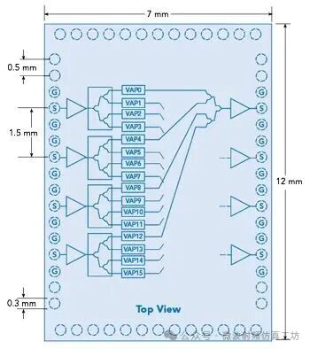
Figure 1 Block diagram of the BFIC chip in BGA package (not to scale).
Modern phased array systems utilize beamformer integrated circuits (BFICs), which typically feature multiple parallel paths on the chip, with independent control over gain and phase for each path. A common BFIC configuration connects two or more RF paths to pins located on the same edge and/or corner of the integrated circuit package. Figure 1 shows a four-input, four-output 16-channel BFIC, with all four inputs located on the same edge of the integrated circuit package. This device architecture is applied in Analog Devices’ ADAR3000/1/6/7 series Ku-band and Ka-band BFICs. Each device features four inputs, four cross-coupled outputs, and a complex digital control system that includes a command processor, on-chip RAM, and FIFO memory.
The complexity and size of BFICs present numerous challenges. The large number of RF inputs and outputs, along with their associated ground-signal-ground configurations, result in very tight pin spacing. Routing multiple RF traces from these closely spaced pins to adjacent circuits or other printed circuit boards (PCBs) is a challenge. RF power attenuation is widely used to reduce sidelobes, but this can lead to power differences between channels of up to 30 dB, making inter-channel isolation critical, and the routing of RF traces significantly affects isolation. In addition to routing issues, transmission line impedance is also very important. Poor transmission line impedance accuracy and inadequate impedance transitions between circuit boards can lead to signal reflections and reduce RF power transmitted to the antenna. Larger signal reflections can also cause instability and oscillation.
This article will explore how to design high-precision RF PCB transmission lines with excellent return loss and isolation in a high-density, high-channel-count multi-board environment. While the focus will be on back-end integrated circuits (BFICs) and phased array applications, the conclusions are equally applicable to any high-frequency circuit design with stringent inter-channel isolation and impedance matching requirements. Additionally, this article covers the important topic of design for manufacturability.
RF Transmission Line Manufacturing
PCB manufacturers support various commonly used RF transmission line topologies, including microstrip, grounded coplanar waveguide (GCPW), stripline, and the less common embedded GCPW (a hybrid of GCPW and stripline). Microstrip is relatively easy to manufacture, but due to its higher trace loss and poorer mode suppression, it is not commonly used at frequencies above 6 GHz. 1 GCPW, embedded GCPW, and stripline perform better at frequencies above 6 GHz due to lower radiation losses and better mode suppression. Embedded transmission line topologies can improve isolation but are more challenging to manufacture and require via connections. These vias are often blind vias to minimize parasitic inductance, which increases the cost of the circuit board.
Figure 2 shows the cross-sections of GCPW, embedded GCPW, and stripline, along with the important geometric parameters that determine the nominal line impedance. These geometric parameters include line width (W1/W2/W3), the lateral distance from the line edge to the adjacent ground plane (G1/G2/G3), the thickness of the dielectric material (T1/T2), and the relative permittivity of the dielectric material (εR1 / εR2 ). Figure 2 does not show the thickness of the copper used for the traces or the required ground via fence. While copper thickness is indeed a consideration, it is a secondary factor. The choice of topology depends on acceptable trace loss, frequency, required inter-line isolation, available space, and the dielectric thickness of the PCB material.

Figure 2 Cross-sections of GCPW, embedded GCPW, and stripline topologies.
How Manufacturing Tolerances Affect Line Impedance
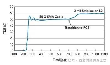
Figure 3 TDR plot of a 3 mil wide stripline on 2 layers.
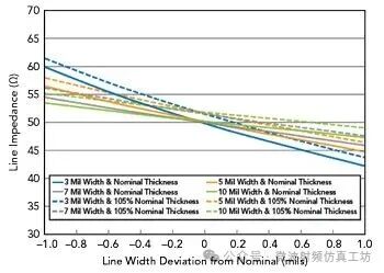
Figure 4 Relationship between line impedance and line width deviation.
Manufacturing tolerances can affect the accuracy of RF line topologies. Figure 3 shows a time-domain reflectometer (TDR) plot of a 3 mil wide stripline designed for 50 Ω impedance, with a measured impedance of approximately 60 Ω. The initial target tolerance was ± 10% (45 to 55 Ω), resulting in a return loss exceeding 20 dB.
Many PCB manufacturers offer trace widths as low as 3 mil (copper foil thickness is also a factor), with tolerances of 1 to 2 mil. 2,3,4Dielectric material manufacturers typically only provide typical dielectric thicknesses, likely because PCB manufacturers determine the final thickness during the board lamination process. If the ground layer does not terminate where it should, the lateral gap to ground may vary. Additionally, if the line width changes, the effective lateral gap width will also change.
Microstrip and stripline RF traces have larger lateral gaps in their designs, which do not affect line impedance. Therefore, for microstrip topologies, all field lines direct to the lower ground plane; for stripline topologies, all field lines direct to both upper and lower ground planes. However, for GCPW RF traces, the lateral gap to the ground plane is designed to be smaller, resulting in most field lines directing to the lateral ground plane.
Figure 4 plots the line impedance of RF stripline traces against the deviation of line width from the nominal value. The figure shows nominal line widths of 3, 5, 7, and 10 mils. Additionally, the figure shows the impedance deviation when the dielectric layer thickness is 5% thicker than the nominal value, assuming a stripline copper layer thickness of 0.7 mil and ε R = 3.1.
Note that wider traces exhibit smaller impedance variations, while narrower traces show larger impedance variations for the same absolute width deviation. Therefore, wider nominal trace widths are more resistant to manufacturing deviations. In contrast, when the dielectric layer thickness increases by 5%, the impedance variation is roughly the same, regardless of the nominal trace width. This means that PCB manufacturers must meet the final pressed thickness requirements within a certain tolerance range to achieve the target line impedance tolerance. The emphasis in Figure 4 is on increasing dielectric layer thickness, as observations from many PCB manufacturing batches with different line topologies have shown that line impedance often exceeds or equals the design target value. This leads to a rule of thumb: design line impedance to be a few ohms lower than the target value, especially for narrower line widths (e.g., less than 5 mils). By adopting this approach, the controlled impedance requirements of PCB manufacturers may need to be relaxed. If fine lines must be used due to other design considerations, a reliable PCB manufacturer should be selected. Trust in PCB manufacturers needs to be built gradually through multiple productions or manufacturing test boards containing traces of various widths, aiming to achieve a 50 Ω ± 10% impedance value. Measurements are then taken to determine which trace width is closest to 50 Ω.
GCPW vs. Embedded GCPW
On any PCB, there will be some degree of coupling between adjacent transmission lines. This coupling can be electrical or through electric and magnetic field coupling, leading to finite isolation. The isolation difference between transmission lines on the PCB can cause issues, especially in applications with significant signal level differences. In phased array systems using multi-channel BFICs, parasitic signal coupling can reduce the linearity of the variable amplitude phase (VAP) module gain control function in high attenuation paths when two adjacent channels operate at minimum and maximum attenuation, respectively. This phenomenon was observed on evaluation boards using GCPW transmission lines. Electromagnetic simulations conducted with Keysight RFPro indicate that embedded GCPW transmission lines can improve in-band isolation between lines by 15 dB compared to existing GCPW PCB solutions.
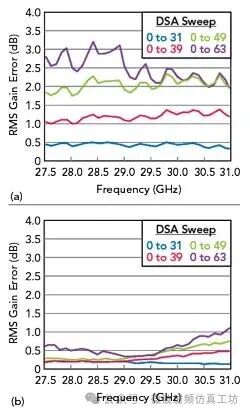
Figure 5 RMS gain error vs. frequency for GCPW (a) and embedded GCPW (b) transmission lines under DSA settings.
Guidelines for Routing Multiple RF Traces
Designing PCB traces for RF beamformers with multiple RF inputs and outputs is a challenge. As mentioned earlier, careful selection and design of transmission line topologies are required. Additionally, proper grounding vias are crucial for achieving good return loss and isolation. Isolation requirements and the geometry of the beamformer integrated circuit (BFIC) determine the choice of transmission line topology. For example, if isolation requirements are around -40 dB, GCPW is a good choice. If isolation of around -65 dB is required, stripline transmission lines should be used based on experimental results.
Next, consider the geometry of the BFIC, focusing on the size of each pin, pin spacing, and the distance between RF pins. For example, consider a BGA with a ball diameter of 5.5 mil (0.22 mm), a pin pitch of 10 mil (0.4 mm), an RF pin spacing of 30 mil (1.2 mm), and an isolation requirement of -65 dB. In this case, a suitable choice is a symmetric stripline with a line width of approximately 6 mil, a dielectric layer thickness of about 6 mil (above and below), and a lateral ground gap of 10 mil, assuming a dielectric constant of around 3. The rule of thumb for stripline is that the lateral ground gap should be about twice the line width, as smaller gaps can affect line impedance. The smaller the distance between RF pins, the narrower the required line width; conversely, the larger the distance between RF pins, the wider the required line width. The latter is preferable as it is more likely to achieve a 50 Ω resistance value during manufacturing.
Routing Near Devices
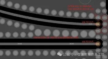
Figure 6 Ground wall vias extending around the transmission lines.
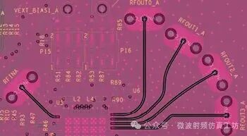
Figure 7 Fan-out of multiple RF outputs.
When using stripline, extra care must be taken during the transition to the top layer device pins, as this transition area can significantly reduce isolation if proper grounding vias are not used. To achieve the highest isolation, the grounding wall of the vias should extend around the end of the stripline at the device transition, as shown in Figure 6. This method extends the critical grounding wall required for optimal isolation performance. The device should also have grounding pins, bumps, and/or pads surrounding the signal pins, and these grounding pins, bumps, and/or pads should roughly align with the extended grounding wall vias.
RF pins that are close to each other may not provide enough area for each transmission line to maintain the same via isolation as with the device. Depending on the available area, typical options for via isolation include:
·Use smaller vias if they do not violate the manufacturer’s aspect ratio rules for dielectric thickness.
·If a line lacks a via at the device interface without compromising isolation, stagger the vias in a moderate area.
·As shown in Figure 6, use a row of larger vias between each line while maintaining the same edge distance as with smaller vias to optimize isolation performance.
·When space between lines is very limited, a row of vias of the same size can be used.
When and how to fan-out traces depends on the relative positions of the RF input/output pins on the device. Generally, fan-out should occur as soon as possible to minimize parallel traces and maximize isolation. As shown in Figure 6, fan-out can occur immediately due to the position of the RF pins. However, Figure 7 shows the fan-out situation of four outputs at different parallel trace distances. In this case, the fan-out is limited by the non-RF input/output routing and associated circuits (L2, L4, P15, P16, etc.) shown at the top of the device and the RF outputs on the right side of the device.
Board Interconnections
The RF impedance discontinuity between RF transmission lines and RF connectors is as important as the transition of traces to the device. There are two physical interconnection schemes for transitioning between different circuit boards:
·Edge-mounted connectors installed laterally at the PCB edge
·Vertically mounted connectors on the PCB.
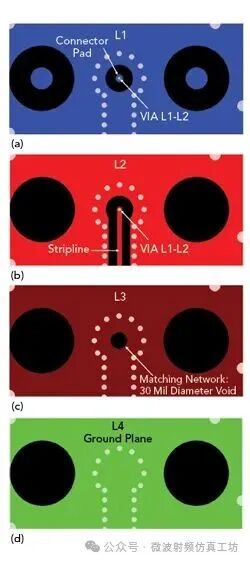
Figure 8 (a) Ground layer, pads, and vias on layer 1. (b) Stripline on layer 2. (c) 30 mil gap matching network on layer 3. (d) Solid ground layer on layer 4.
Both types provide SMA, SMP, SMPM, 2.92 mm, and 2.4 mm interfaces.
The choice between edge-mounted and vertical connectors is greatly influenced by the device’s form factor. Edge-mounted connectors imply lateral interconnections of the PCB. This arrangement may be optimal if the system is housed in a single metal chassis/heatsink. Vertical connectors allow for stacking multiple circuit boards. This can achieve a more compact form factor, but since a single circuit board typically lacks a heatsink, this configuration may require airflow for cooling. If one circuit board uses an edge-mounted connector while another uses a vertical connector, the circuit boards will connect orthogonally in a slot configuration.
While edge connectors are widely used, they also have potential drawbacks due to their connection at the edge of the circuit board. Edge connectors require the upper ground layer of the PCB (preferably the lower ground layer) to extend to the edge of the circuit board. Most PCB manufacturers can only guarantee a 2 mil distance between the edge of the ground layer at the connector location and the edge of the circuit board when using standard edge milling/wiring and etching back techniques. This can lead to impedance discontinuities, as the lack of a ground return loop in a gap of 2 mil or greater reduces return loss.
Since vertical connectors are not constrained by the edge of the circuit board, they are not affected by edge routing issues. On simple single-device circuit boards, connectors can be placed close to the device to minimize insertion loss. Additionally, impedance matching can be performed on the transition sections of the circuit board to minimize impedance discontinuities. Some connector suppliers customize connector packages based on specific trace designs and stack-up structures. Figure 8 shows the four-layer PCB structure of a vertical connector from SV Microwave interfacing with stripline RF traces.
A significant challenge with vertical connectors is achieving good alignment between the connector and the PCB pads during assembly. Ideally, the center pin of the connector should align with the center of the circular pad on the PCB. However, when the connector is mounted on a two-dimensional ground plane, it may shift in both the lateral and longitudinal directions. Movement in either direction can misalign the center pin with the PCB pad. The best alignment method is to strictly control the size of the mounting holes to minimize movement of the connector.
Conclusion
Modern high-frequency board-level RF integrated circuits (BFICs) present greater challenges for PCB design. To maintain high inter-channel isolation, some RF trace designs have had to shift from surface-level GCPW (graphene sheet coplanar waveguide) to embedded stripline. Even with embedded stripline, care must be taken to use tightly spaced via fences to maintain isolation between adjacent traces, with these via fences fully surrounding the device pins. In designing these challenging traces, PCB designers can proactively prevent potential manufacturing issues by avoiding the use of excessively fine RF traces or designing characteristic impedances slightly lower than the target values. When designing board interconnections, the choice between top-mounted or edge-mounted interconnections is often based on the size of the end device. Top-mounted interconnections are less affected by the manufacturing processes at the edges of the circuit board.