In embedded development, there is a crucial yet often overlooked “invisible tool”—the JTAG interface. It is embedded within chips, supporting core operations such as debugging and programming, and developers typically interact with it through IDEs without delving into the underlying details.
However, as devices trend towards miniaturization and high integration, the pin and wiring requirements of traditional JTAG have become a hindrance. The emergence of cJTAG aims to break this deadlock, adapting to new demands with a more streamlined design and bringing new possibilities for embedded debugging.
 From JTAG to cJTAG: The Evolution of Embedded Debugging Interfaces
In the world of embedded development, the JTAG (Joint Test Action Group) interface is crucial yet often ignored. Most developers interact with it through IDEs and debugging tools without needing to focus on the underlying protocol; in final products, the JTAG interface is usually not used as a functional interface.
Since its inception, the JTAG interface has been deeply embedded in almost every complex chip. It serves as a bridge for engineers to connect to the digital hardware world and is a core technical means for chip debugging, program programming, and boundary scan testing.
JTAG has defined the standard for embedded debugging with its powerful capabilities. The standard 4-wire (TDI, TDO, TMS, TCK) or 5-wire (adding TRST) Test Access Port (TAP) has become a standard feature for countless development boards and debuggers.
The Test Access Port (TAP) is a standardized interface for testing logic, consisting of 4 mandatory pins + 1 optional pin.
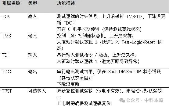
However, as electronic devices and chips develop towards miniaturization and high integration, the limitations of the traditional JTAG architecture have become apparent. At the chip level: it occupies too many precious I/O pins, putting resource pressure on microcontrollers and IoT chips with limited pin counts; at the board level: it requires additional wiring space and connectors, increasing PCB complexity and cost.
These challenges have created a demand for a new generation of debugging interface standards. cJTAG (Compact JTAG), based on the IEEE 1149.7 standard, achieves an architectural innovation for debugging interfaces through protocol optimization and pin multiplexing technology while maintaining full backward compatibility.
 The Birth of cJTAG Aims to Solve Two Core Issues
▋ “Reduction” —— In the face of miniaturized chips and compact PCBs, the traditional 4/5-wire interface of JTAG appears increasingly “luxurious”. The primary goal of cJTAG is to significantly reduce the physical pin and wiring space requirements of the debugging interface, cutting it down from 4 or 5 wires to just 2 wires (commonly named TCKC and TMSC), clearing the way for product “miniaturization” and “cost reduction”.
▋ “Compatible” —— While reducing pins, it also ensures complete backward compatibility with the traditional JTAG (IEEE 1149.1) standard. This compatibility means that debuggers supporting cJTAG can operate traditional JTAG devices, and cJTAG devices can also be recognized by traditional JTAG debuggers (though their advanced features cannot be used).
cJTAG (IEEE 1149.7) is a complement and evolution of the traditional JTAG standard. The core mission of the working group is not to start from scratch but to establish a more efficient and flexible new standard based on the existing JTAG functionality while addressing the pain points of modern chip systems.
 Working Modes and Implementation of cJTAG
So how does cJTAG achieve “reducing from 4 or 5 wires to just 2 wires” while ensuring “complete backward compatibility”? Traditional JTAG communication can be viewed as a simple logic of “bit manipulation”, while cJTAG introduces a more complex concept of “packetization”. It packages instructions, data, and control information into standard “data packets” and transmits them through a shared communication line (TMSC). This packet-based communication method is the fundamental reason it can maintain its original functionality while reducing the number of cables.
In cJTAG mode, the three signals that originally needed to be transmitted separately through the JTAG interface—TMS, TDI, and TDO on the device side—are multiplexed onto the bidirectional signal of cJTAG’s TMSC, which is uniformly transmitted to the debugging tool. This is the core technology that allows cJTAG to simplify 4/5 pins to 2 pins.
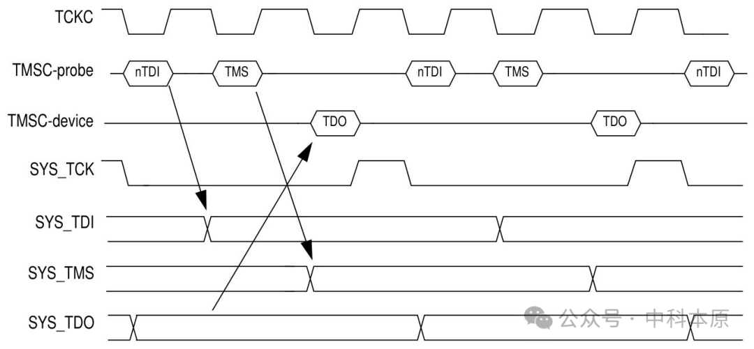
According to the IEEE 1149.7 standard, in the Oscan1 format, every 3 TCKC pulses constitute a “scan packet” (SP). The transmission order of the 3 signal bits in the packet is fixed: the 1st bit: nTDI, which is the inverse signal of TDI, used to carry the reverse information of the test data input; the 2nd bit: TMS, used to carry the test mode selection instruction; the 3rd bit: TDO, used to carry the test data output information.
Executing a “1-bit JTAG scan” (i.e., transmitting 1 bit of debug data) requires 3 TCKC pulses, unlike the traditional JTAG where 1 clock pulse transmits 1 bit. This is because the multiplexed signals need to be distinguished by multiple clock cycles. Similarly, to avoid signal conflicts, the driving rights of TMSC are divided by clock cycles: the first 2 TCKC bit cycles (corresponding to nTDI and TMS transmission) are driven by the debugging tool to send control information and input data to the device side; the last TCKC bit cycle (corresponding to TDO transmission) is driven by the device to return output data to the debugging tool.
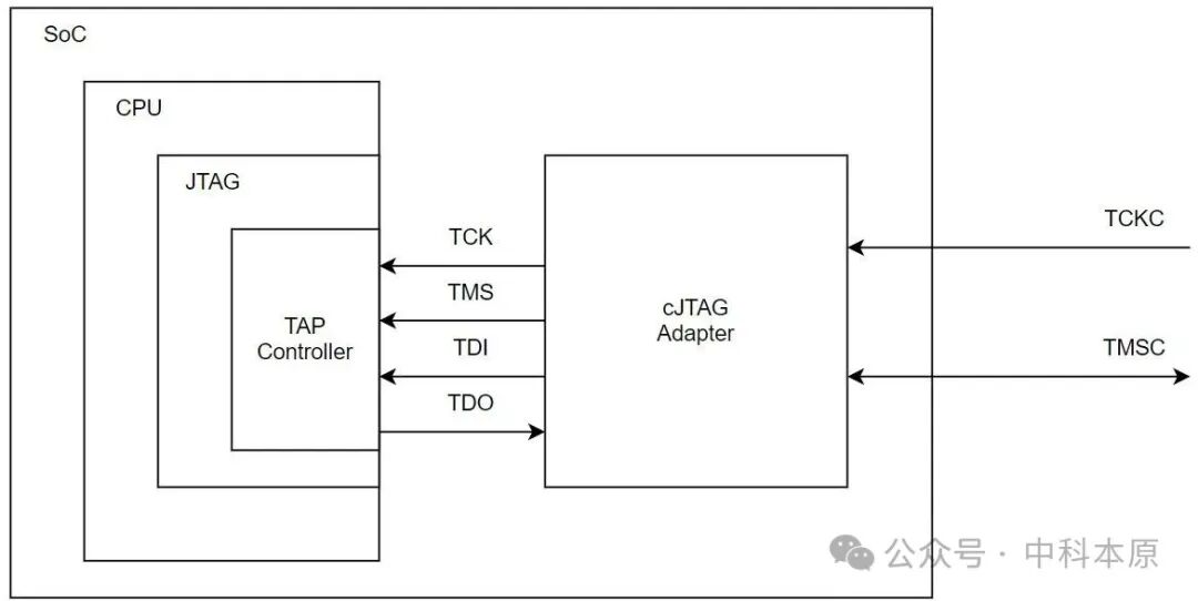
The above figure presents a typical design scheme, visually demonstrating how to quickly integrate cJTAG functionality into an existing JTAG system-on-chip (SoC) through a cJTAG Adapter.
This scheme does not require reconstructing or replacing the existing traditional JTAG core logic within the SoC; the cJTAG Adapter merely serves as an “intermediate conversion layer”, directly reusing the original 4-wire JTAG interface to connect with the TAP controller. This means there is no need to redevelop the underlying hardware modules related to JTAG, allowing the use of mature traditional JTAG design solutions, reducing R&D risks, and shortening validation cycles. At the same time, it addresses the core pain points of traditional 4/5-wire JTAG, significantly alleviating the pressure on devices with “pin resource constraints” such as microcontrollers (MCUs) and IoT chips, leaving space for products to integrate more functional modules (such as sensors and external storage units).
 From JTAG to cJTAG: A Profound Evolution from “Signal Level” to “Protocol Level”
cJTAG cleverly resolves the contradiction between hardware resources and debugging needs through packetization and protocol layering. True innovation does not necessarily mean a complete overhaul; it can also be a precise optimization and enhancement of the classics.
For engineers, understanding cJTAG means mastering a more efficient debugging key. In fields such as IoT devices, wearable electronics, and automotive chips, where space and cost are extremely sensitive, this technology will gradually transition from an “optional” to a “mandatory” choice. It reminds us that while pursuing functional innovation, continuous optimization of the underlying infrastructure is also an indispensable force driving technological progress.
 Previous Recommendations
Zhongke Benyuan is about to launch the RISC-V architecture FDM-RV0025

The Art of Code Partitioning: How Dual-Area Architecture Balances Security and Performance?

Design and Implementation of Dual PMSM Control Scheme Based on FDM320RV335