This week, in the latest issue of the prestigious journal Science, Shanghai Jiao Tong University and Zhejiang University have made significant progress in semiconductor materials research. Let’s take a closer look at each of their achievements:On the evening of March 13, 2025, a collaborative team including Shi Zhiwen, Liang Qi, and Chen Jiajun from Shanghai Jiao Tong University, Ouyang Wengen from Wuhan University, Jin Chuanhong from Zhejiang University, and Zhang Guangyu from the Institute of Physics, Chinese Academy of Sciences, published their latest research findings in Science as a joint communication under the title First Release. The study reports on chiral carbon nanotube van der Waals crystals. It details the direct growth of densely packed arrays of single-walled carbon nanotubes on a hexagonal boron nitride (hBN) substrate, with each array exhibiting highly ordered and uniform chirality. Molecular dynamics simulations indicate that this self-assembly growth mechanism is driven by the van der Waals forces between the tubes and the extremely low sliding friction of single-walled carbon nanotubes on the atomically flat hBN substrate. Field-effect transistors fabricated from the grown single-walled carbon nanotube arrays demonstrate high performance at room temperature, with a mobility of up to 2000 cm²/V·s, an on/off ratio of approximately 10⁷, and a maximum current density of about 6 mA/μm. This result marks a significant step forward in the practical application of single-walled carbon nanotubes in nanoelectronic devices and circuits, and the growth mechanism proposed in this study provides a method for fabricating complex nanostructures, which is particularly significant for the development of new van der Waals materials.In summary, this research has developed a novel method for fabricating carbon nanotube arrays, successfully achieving the direct growth of a single-chirality parallel densely packed carbon nanotube array, and for the first time obtaining a carbon nanotube van der Waals crystal structure. The study not only addresses key challenges in the application of carbon nanotubes in integrated circuits but also demonstrates the enormous potential of the fabricated single-chirality densely packed carbon nanotube arrays for future high-performance carbon-based nanoelectronic chip applications, paving new pathways for the application of carbon nanotube materials in electronic devices.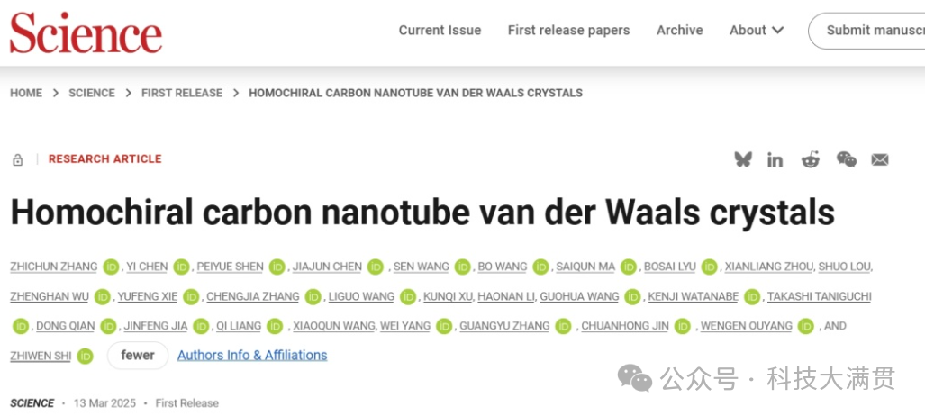 The first completing unit of this article is Shanghai Jiao Tong University, with the first corresponding author being Shi Zhiwen from the School of Physics and Astronomy at Shanghai Jiao Tong University. He graduated with a bachelor’s degree from University of Science and Technology of China in 2007 and obtained his Ph.D. from the Institute of Physics, Chinese Academy of Sciences in 2012. After completing his Ph.D., he conducted postdoctoral research at the University of California, Berkeley, and returned to China in 2016, joining Shanghai Jiao Tong University, where he is currently a professor in the School of Physics and Astronomy. Shi Zhiwen primarily engages in experimental condensed matter physics research, focusing on low-dimensional materials and devices, near-field optics, laser spectroscopy, electrical transport, and scanning probe microscopy characterization. Notably, last March, he reported in the top journal Nature as the first corresponding author on the growth of graphene nanoribbons in hBN stacks for high-performance electronic products, achieving the embedded growth of single-chirality ultra-long graphene nanoribbons between boron nitride layers.
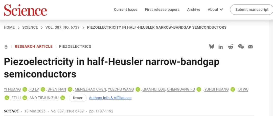
 In the same issue of Science, a collaborative team from Zhejiang University, including Zhu Tiejun, Fu Chenguang, and Huang Yuhui, published their latest research findings. This study reports on the piezoelectric effect in half-Heusler narrow bandgap semiconductors.The research details observations of the piezoelectric (PE) effect in half-Heusler (HH) narrow bandgap semiconductors such as titanium nickel tin (TiNiSn), zirconium nickel tin (ZrNiSn), and titanium cobalt antimony (TiCoSb). The shear piezoelectric strain coefficients of TiNiSn, ZrNiSn, and TiCoSb are approximately 8 pC/N, 38 pC/N, and 33 pC/N, respectively. Among these, the shear piezoelectric strain coefficients of ZrNiSn and TiCoSb represent very high values for non-centrosymmetric non-polar materials. The study showcases a piezoelectric sensor based on TiCoSb, which exhibits a large voltage response and is capable of charging capacitors. The piezoelectric effect in half-Heusler (HH) materials remains thermally stable below 1173 Kelvin, indicating its potential for high-temperature applications. In summary, this research is the first to observe the piezoelectric effect in half-Heusler narrow bandgap semiconductor materials, suggesting that half-Heusler narrow bandgap semiconductors may have broad application prospects in advanced multifunctional technologies and could provide new insights for the design of novel piezoelectric materials and transduction technologies.
 The first corresponding author of this article is Zhu Tiejun from Zhejiang University, who obtained his bachelor’s, master’s, and doctoral degrees from Zhejiang University from 1992 to 2001. After completing his Ph.D., he conducted postdoctoral research at the Singapore-MIT Alliance and returned to Zhejiang University in 2004, where he is currently a distinguished professor and the dean of the School of Materials Science and Engineering. Notably, just last month, Zhu Tiejun and his collaborators reported in the Nature sub-journal Nature Materials on achieving inorganic semiconductor-like metal processing deformation through iterative sublattice amorphization.