InP-based semiconductor lasers are widely used in fiber optic communication, data centers, 5G networks, satellite communication, and laser radar due to their advantages such as low fiber transmission loss, minimal external environmental interference, and safety for human eyes. Recently, the nano processing platform at Suzhou Nano Institute has made significant progress in the field of InP-based semiconductor lasers based on its accumulation in InP material epitaxy, device design, and device fabrication.
Progress 1: Low Threshold High Power Single-Mode LaserDFB lasers have become the core laser source for systems such as fiber optic communication, data center optical switching, and 5G networks due to their narrow linewidth, high side mode suppression ratio, and low phase noise. Reducing the threshold is crucial for enhancing energy efficiency and integration. By employing an asymmetric coupled grating structure, the mirror symmetry is broken to couple odd and even modes, forming a fourth-order band edge degenerate state to enhance the local photon state density, effectively reducing the threshold current. The fabricated device achieved stable single longitudinal mode output at 1550 nm, with the threshold current density reduced from 2.41 kA/cm² to 1.88 kA/cm² (a reduction of 22%), while maintaining a high power output of over 90 mW.The related results were published in Optics Express under the title Degenerate band edge laser with enhanced local density of optical states for threshold reduction, with PhD student Guo Yujun as the first author, and Sun Tianyu and Zou Yonggang as corresponding authors.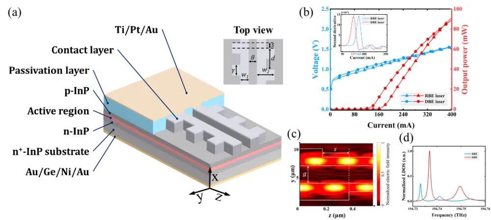 Figure 1. Band edge degenerate laser (a) structural schematic; (b) LIV characteristics; (c) electric field distribution; (d) local optical state densityProgress 2: Ultra-Broadband Passively Mode-Locked LaserSemiconductor passively mode-locked lasers are core demands in microwave photonics, analog-to-digital conversion, optical communication, laser radar, and optical computing systems, with their spectral bandwidth directly determining pulse width, supported transmission capacity, and modulation freedom. By designing a multi-quantum well material system with gradient components, the gain spectrum top was significantly broadened while remaining flat, combined with a two-section cavity structure optimization, achieving a -3dB bandwidth exceeding 20nm and a -10dB bandwidth exceeding 35nm for passively mode-locked laser output. To date, these two bandwidth metrics are the maximum for communication band electrically pumped passively mode-locked lasers. Additionally, this device features a simple structure, stable mode-locking state, good repeatability, and process compatibility, making it easy to scale up production.The research results were published in Optics Letters under the title Beyond 20 nm frequency comb generation through a two-section quantum well passively mode-locked semiconductor laser, with PhD student Qin Bisheng as the first author, and Sun Tianyu and Zhang Ruiying as corresponding authors.
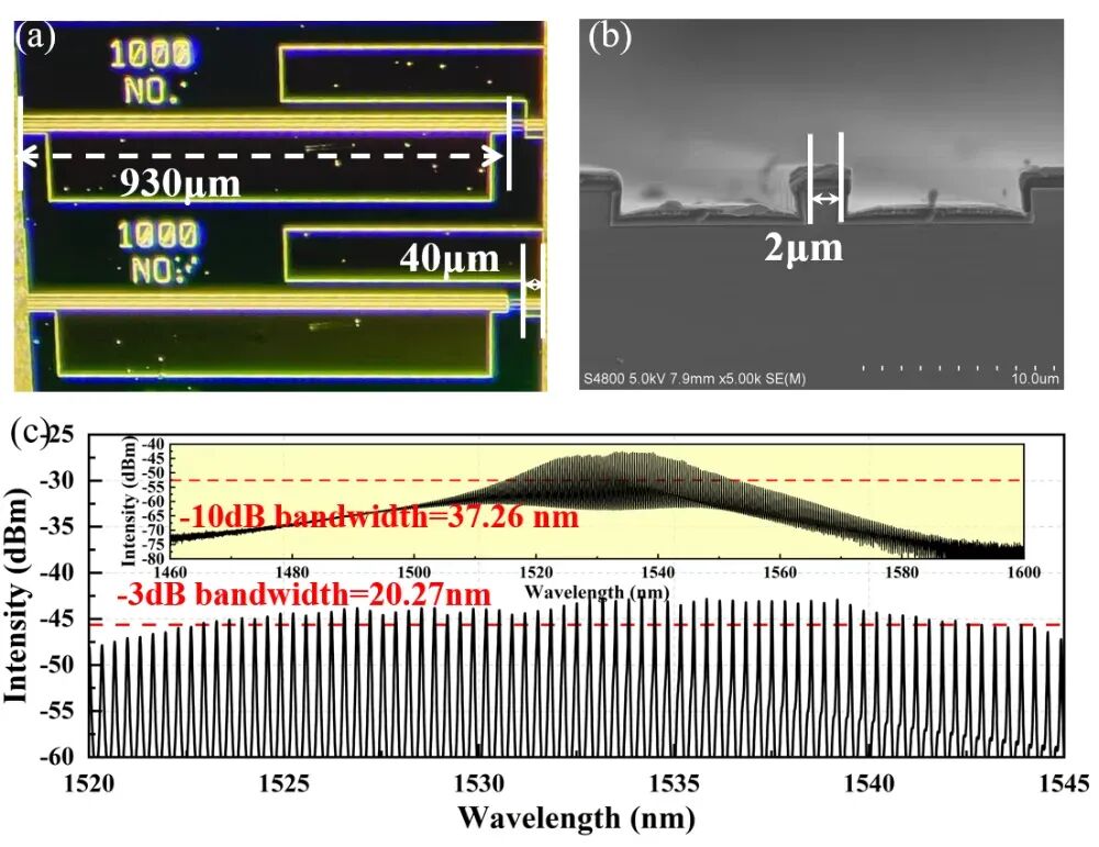 Figure 2. (a) Optical micrograph of the two-section passively mode-locked laser; (b) device cross-section SEM image; (c) output spectrumProgress 3: High-Efficiency Integrable Laser Source Based on InPInP-based monolithic photonic integration can fully leverage the active and high-frequency performance of InP materials, making it highly sought after in coherent communication transceivers, satellite communication payloads, and RF front ends. However, the existing semiconductor laser process involves oscillation amplification of stimulated radiation through dissociated cavity faces. To meet the on-chip laser source requirements for InP-based photonic integrated circuits, a multi-depth etching process was employed to complete the fabrication of waveguides and end faces in one step, combined with SiO₂ passivation layers and Au high-reflective coatings, achieving a rear end face reflectivity greater than 97% and a front end face reflectivity lower than 9%, obtaining power output comparable to traditional processes under CW conditions.The related research results were published in IEEE Photonics Technology Letters under the title Continuous-wave operation of InP laser with etched facet mirrors for photonic integrated circuits, with Xing Zheng as the first author, and Sun Tianyu and Zhang Baoshun as corresponding authors.
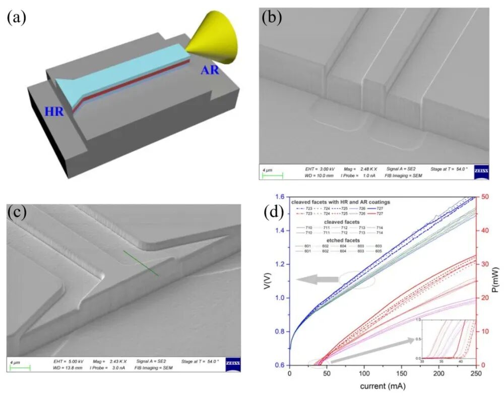 Figure 3. (a) Schematic diagram of dry-etched end face laser structure; (b) AR end face SEM image; (c) HR end face SEM image; (d) Performance comparison of etched end face laser and natural cleaved laserThe above work was supported by the National Key R&D Program and other projects.